

NTE NTE2378 Datasheet
NTE2378
MOSFET
N–Channel Enhancement Mode,
High Speed Switch
Description:
The NTE2378 is an N–Channel Enhancement Mode Power MOS Field Effect Transistor. Easy drive
and very fast switching times make this device ideal for high speed switching applications. Typical
applications include switching mode power supplies, uninterruptible power supplies, and motor
speed control.
Features:
D Low ON–State Resistance
D Very High–Speed Switching
D Converters
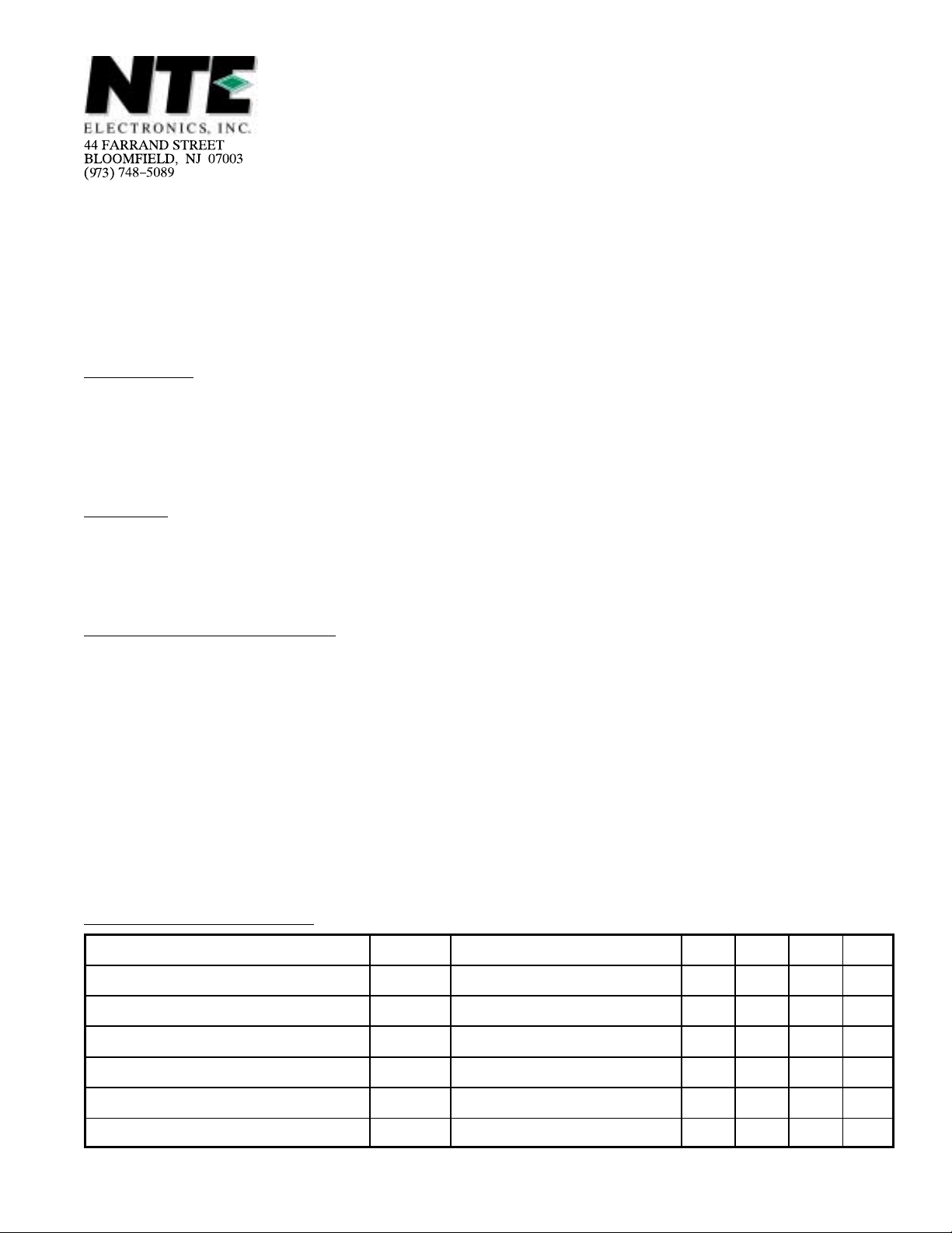
Absolute Maximum Ratings:
Drain–Source Voltage, V
Gate–Source Voltage, V
DC Drain Current, I
DSS
GSS
D
Pulsed Drain Current (Note 1), I
Allowable Power Dissipation (T
Maximum Channel Temperature, T
Storage Temperature Range, T
(TA = +25°C)
DP
= +25°C), P
C
ch
stg
900V. . . . . . . . . . . . . . . . . . . . . . . . . . . . . . . . . . . . . . . . . . . . . . . . . . . . . . . .
±30V. . . . . . . . . . . . . . . . . . . . . . . . . . . . . . . . . . . . . . . . . . . . . . . . . . . . . . . .
5A. . . . . . . . . . . . . . . . . . . . . . . . . . . . . . . . . . . . . . . . . . . . . . . . . . . . . . . . . . . . . . . . .
10A. . . . . . . . . . . . . . . . . . . . . . . . . . . . . . . . . . . . . . . . . . . . . . . . . . . .
D
120W. . . . . . . . . . . . . . . . . . . . . . . . . . . . . . . . . . . . . . .
+150°C. . . . . . . . . . . . . . . . . . . . . . . . . . . . . . . . . . . . . . . . . . . . . . .
–55° to +150°C. . . . . . . . . . . . . . . . . . . . . . . . . . . . . . . . . . . . . . . . . .
Note 1. Pulse Width ≤ 10µs, Duty Cycle ≤ 1%.
Note 2. Be careful in handling the NTE2378 because it has no protection diode between gate and
source.
Electrical Characteristics:
Parameter Symbol Test Conditions Min Typ Max Unit
Drain–Source Breakdown Voltage V
Zero–Gate Voltage Drain Current I
Gate–Source Leakage Current I
Cutoff Voltage V
(TA = +25°C unless otherwise specified)
(BR)DSSID
DSS
GSS
GS(off)VDS
= 1mA, VGS = 0 900 – – V
VGS = 0, VDS = 900V – – 1.0 mA
VDS = 0, VGS = ±30V – – ±100 nA
= 10V, ID = 1mA 2 – 3 V
Static Drain–Source On Resistance R
Forward Transconductance g
DS(on)VGS
= 10V, ID = 2A – 2.8 3.6 Ω
VDS = 20V, ID = 2A 1.0 2.0 – mho
fs
Electrical Characteristics (Cont’d): (TA = +25°C unless otherwise specified)
Parameter Symbol Test Conditions Min Typ Max Unit
Input Capactiance C
Output Capacitance C
Reverse Transfer Capactiance C
Turn–On Time t
d(on)
Rise Time t
Turn–Off Delay Time t
d(off)
Fall Time t
Diode Forward Voltage V
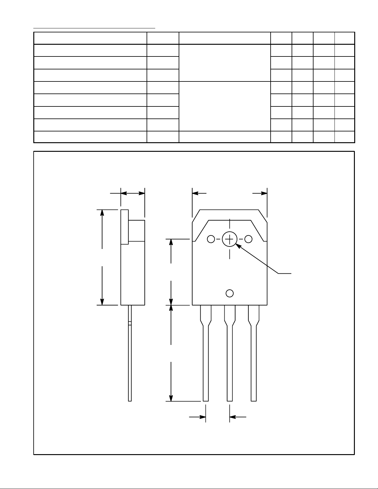
.190 (4.82)
iss
oss
rss
r
f
SD
– 700 – pf
VDS = 20V, f = 1MHz
– 300 – pf
– 170 – pf
– 15 – ns
VDD = 200V, ID = 2A,
VDD = 200V, ID = 2A,
= 10V, RGS = 50Ω
V
GS
– 35 – ns
– 200 – ns
– 65 – ns
IS = 5A, VGS = 0 – – 1.8 V
.615 (15.62)
.787
(20.0)
.591
(15.02)
.787
(20.0)
D
.126
(3.22)
Dia
GDS
.215 (5.47)
 Loading...