

NTE NTE2317 Datasheet

NTE2317
Silicon NPN Transistor
High Voltage Fast Switching Power Darlington
Description:
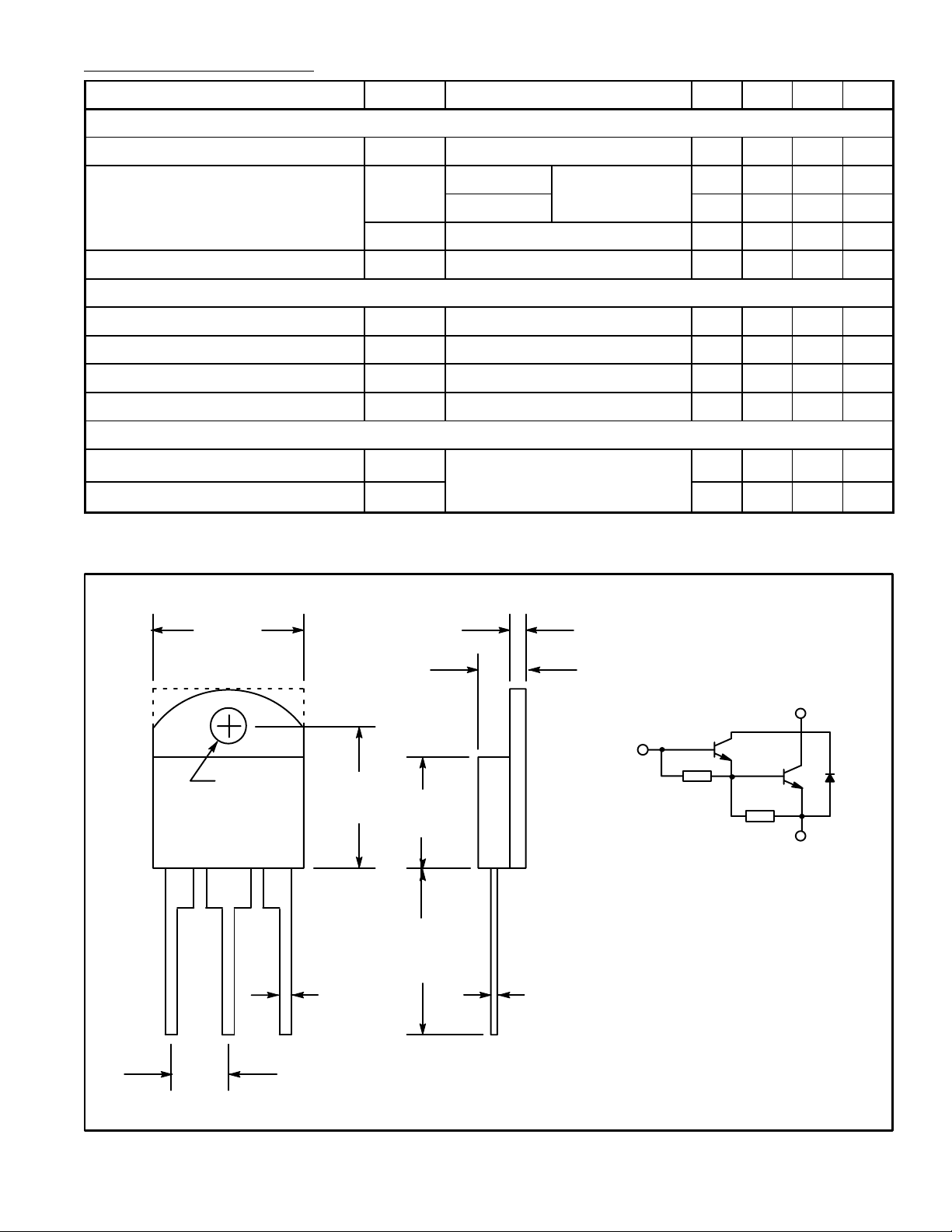
The NTE2317 is a multiepitaxial bipolar NPN transistor in a monolithic Darlington configuration
mounted in a TO218 type package designed for use in automotive ignition applications and inverter
circuits for motor controls. Controlled performances in the linear region make this device particularly
suitable for car ignitions where current limiting is achieved desaturing the darlington.
Features:
D High Performance Electronic Ignition Darlington
D High Ruggedness
Applications:
D Automotive Market
Absolute Maximum Ratings:
Collector–Emitter Voltage (VBE = 0), V
Collector–Emitter Voltage (I
Emitter–Base Voltage (I
Collector Current, I
C
B
= 0), V
C
= 0), V
EBO
CES
CEO
Continuous 15A. . . . . . . . . . . . . . . . . . . . . . . . . . . . . . . . . . . . . . . . . . . . . . . . . . . . . . . . . . . . . . . . . .
Peak (t
Base Current, I
≤ 10ms) 30A. . . . . . . . . . . . . . . . . . . . . . . . . . . . . . . . . . . . . . . . . . . . . . . . . . . . . . . . . . . . .
p
B
Continuous 1A. . . . . . . . . . . . . . . . . . . . . . . . . . . . . . . . . . . . . . . . . . . . . . . . . . . . . . . . . . . . . . . . . . .
Peak (tp ≤ 10ms) 5A. . . . . . . . . . . . . . . . . . . . . . . . . . . . . . . . . . . . . . . . . . . . . . . . . . . . . . . . . . . . . .
Total Power Dissipation (T
≤ +25°C), P
C
tot
Maximum Operating Junction Temperature, T
Storage Temperature Range, T
Thermal Resistance, Junction–to–Case, R
stg
thJC
J
–40° to +150°C. . . . . . . . . . . . . . . . . . . . . . . . . . . . . . . . . . . . . . . . . .
500V. . . . . . . . . . . . . . . . . . . . . . . . . . . . . . . . . . . . . . . . . . . .
450V. . . . . . . . . . . . . . . . . . . . . . . . . . . . . . . . . . . . . . . . . . . . . .
5V. . . . . . . . . . . . . . . . . . . . . . . . . . . . . . . . . . . . . . . . . . . . . . . . . . .
125W. . . . . . . . . . . . . . . . . . . . . . . . . . . . . . . . . . . . . . . . . . .
+150°C. . . . . . . . . . . . . . . . . . . . . . . . . . . . . . . . . . . . . .
1°C/W. . . . . . . . . . . . . . . . . . . . . . . . . . . . . . . . . . . . . . .
Electrical Characteristics: (TC = +25°C unless otherwise specified)
Parameter Symbol Test Conditions Min Typ Max Unit
OFF Characteristics
Collector–Emitter Sustaining Voltage V
Collector Cutoff Current I
Emitter Cutoff Current I
CEO(sus)IC
CES
I
CEO
EBO
= 100mA, Note 1 450 – – V
TJ = +25°C
TJ = +125°C
VCE = 500V,
VBE = 0
VCE = 450V, IB = 0 – – 1 mA
IC = 0, VEB = 5V – – 50 mA
ON Characteristics (Note 1)
Collector–Emitter Saturation Voltage V
Base–Emitter Saturation Voltage V
CE(sat)IC
BE(sat)IC
DC Current Gain h
Diode Forward Voltage V
FE
F
= 8A, IB = 150mA – 1.09 1.8 V
= 8A, IB = 150mA – 1.77 2.2 V
IC = 5A, VCE = 10V 300 – –
IF = 10A – 1.43 2.8 V
Switching Characteristics (Switching Times on Inductive Load)
Storage Time t
s
VCC = 12V, VBE = 0, LB = 7mH,
IC = 7A, IB = 70mA, RBE = 47Ω,
Fall Time t
f
V
clamp
= 300V
Note 1. Pulse Test: Pulse Width = 300µs, Duty Cycle = 1.5%.
– – 1 mA
– – 5 mA
– 15 – µs
– 0.5 – µs
.600
(15.24)
C
.156
(3.96)
Dia.
BCE
.216 (5.45)
.173 (4.4)
.550
(13.97)
.055 (1.4)
.060 (1.52)
.430
(10.92)
.500
(12.7)
Min
.015 (0.39)
C
B
800Ω
50Ω
NOTE: Dotted line indicates that
case may have square corners
E
 Loading...