

NTE NTE221 Datasheet
NTE221
MOSFET
Dual Gate, N–Channel for
VHF TV Receivers Applications
Description:
The NTE221 is an N–channel depletion type, dual–insulated gate, field–effect transistor that utilizes
MOS construction. This device has characteristics which makes it highly desirable for use in RF–amplifier applications.
Features:
D Extremely Low Feedback Capacitance
D High Power Gain
Absolute Maximum Ratings:
Drain–to–Source Voltage, V
Gate 1–to–Source Voltage, V
(TA = +25°C unless otherwise specified)
DS
G1S
Continuous (DC) +1V to –8V. . . . . . . . . . . . . . . . . . . . . . . . . . . . . . . . . . . . . . . . . . . . . . . . . . . . . .
Peak AC +20V to –8V. . . . . . . . . . . . . . . . . . . . . . . . . . . . . . . . . . . . . . . . . . . . . . . . . . . . . . . . . . . .
Gate 2–to–Source Voltage, V
Continuous (DC) –8V to 40% of V
G2S
. . . . . . . . . . . . . . . . . . . . . . . . . . . . . . . . . . . . . . . . . . . . . . . .
Peak AC –8V to +20V. . . . . . . . . . . . . . . . . . . . . . . . . . . . . . . . . . . . . . . . . . . . . . . . . . . . . . . . . . . .
Drain–to–Gate Voltage, V
Pulsed Drain Current (Note 1), I
Transistor Dissipation (T
or V
DG1
D
= +25°C), P
A
DG2
T
Derate Linearly Above 25°C 2.67mW/°C. . . . . . . . . . . . . . . . . . . . . . . . . . . . . . . . . . . . . . . . . . . .
Operating Ambient Temperature Range, T
Storage Temperature Range, T
stg
opr
Lead Temperature (During Soldering, 1/32” from seating surface, 10sec max), T
Note 1. Pulse test: Pulse Width ≤ 20ms, Duty Cycle ≤ 15%.
Electrical Characteristics:
Parameter Symbol Test Conditions Min Typ Max Unit
Gate 1–to–Source Cutoff Voltage V
Gate 2–to–Source Cutoff Voltage V
Gate 1 Leakage Current I
Gate 2 Leakage Current I
(TA = +25°C unless otherwise specified)
(off) VDS = 15V, V
G1S
(off) VDS = 15V, V
G2S
G1SS
G2SS
V
V
G1S
G2S
= 20V, V
= 20V, V
= 4V, ID = 200mA – –2 – V
G2S
= 0, ID = 200mA – –2 – V
G1S
= 0, VDS = 0 – – 1 nA
G2S
= 0, VDS = 0 – – 1 nA
G1S
0 to +20V. . . . . . . . . . . . . . . . . . . . . . . . . . . . . . . . . . . . . . . . . . . . . . . . . .
DS
+20V. . . . . . . . . . . . . . . . . . . . . . . . . . . . . . . . . . . . . . . . . . . . . . . .
50mA. . . . . . . . . . . . . . . . . . . . . . . . . . . . . . . . . . . . . . . . . . . . . . . . . . .
400mW. . . . . . . . . . . . . . . . . . . . . . . . . . . . . . . . . . . . . . . . . . .
–65° to +175°C. . . . . . . . . . . . . . . . . . . . . . . . . . . . . . . . .
–65° to +175°C. . . . . . . . . . . . . . . . . . . . . . . . . . . . . . . . . . . . . . . . . .
L
+265°C. . . . . . . .
Electrical Characteristics (Cont’d): (TA = +25°C unless otherwise specified)
Parameter Symbol Test Conditions Min Typ Max Unit
Drain Current I
Forward Transconductance g
DSS
VDS = 13V, V
VDS = 13V, ID = 10mA, V
fs
G1S
= 0, V
= 4V – 18 – mA
G2S
G2S
= 4V,
– 1000 – µmhos
f = 1kHz
Performance Characteristics: (TA = +25°C, f = 200MHz, Note 2 unless otherwise specified)
Parameter Symbol Test Conditions Min Typ Max Unit
Small–Signal, Short Circuit Reverse
Transfer Capacitance
Output Capacitance C
Input Capacitance C
Input Resistance r
Output Resistance r
Magnitude of Forward Transconductance |Yfs| – 11000 – µmhos
Phase Angle of Forward Transadmittance – –46 – deg
Maximum Available Power Gain MAG – 20 – dB
Maximum Usable Power Gain
(Unneutralized)
Power Gain G
Noise Figure NF – – 5 dB
C
oss
iss
oss
(Drain–to–Gate 1) at f = 1MHz – 0.02 0.03 pF
rss
– 2.2 – pF
iss
– 5.5 – pF
– 1.2 – kΩ
– 2.8 – kΩ
MUGuNote 3 – 20 – dB
PS
– 17.5 – dB
Note 2. V
is adjusted for ID = 10mA, Gate 2 at AC ground potential, VDS = 13V, V
G1S
Note 3. Limited by practical design considerations.
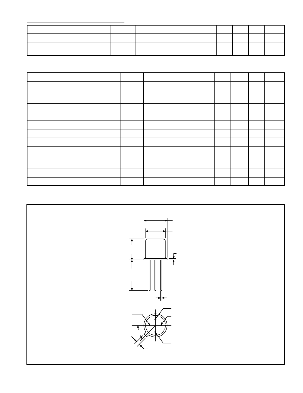
.190
(4.82)
.500
(12.7)
Min
.018 (0.45) Dia
Drain
45°
.220 (5.58) Dia
.185 (4.7) Dia
.030 (.762)
Gate 2
Gate 1
G2S
= 4V.
.040 (1.02)
Source/Case
 Loading...