

NTE NTE215 Datasheet
NTE215
Silicon NPN Transistor
Darlington Driver
Description:
The NTE215 is a silicon NPN Darlington transistor in a TO3P type package. Typical applications include motor drivers, printer hammer drivers, relay drivers, regulated DC power supply controllers.
Features:
D High DC Current Gain
D Large Current Capacity and Wide ASO
D Low Saturation Voltage
Absolute Maximum Ratings:
Collector to Base Voltage, V
Collector to Emitter Voltage, V
Emitter to Base Voltage, V
Collector Current, I
C
(TA = +25°C unless otherwise specified)
CBO
CEO
EBO
Continuous 8A. . . . . . . . . . . . . . . . . . . . . . . . . . . . . . . . . . . . . . . . . . . . . . . . . . . . . . . . . . . . . . . . . . .
Peak 12A. . . . . . . . . . . . . . . . . . . . . . . . . . . . . . . . . . . . . . . . . . . . . . . . . . . . . . . . . . . . . . . . . . . . . . .
Collector Dissipation (T
Collector Dissipation (T
Operating Junction Temperature, T
Storage Temperature Range, T
Electrical Characteristics:
Parameter Symbol Test Conditions Min Typ Max Unit
Collector Cutoff Current I
Emitter Cutoff Current I
DC Current Gain h
Current Gain–Bandwidth Product f
Collector–Emitter Saturation Voltage V
Base–Emitter Saturation Voltage V
Collector–Base Breakdown Voltage V
Collector–Emitter Breakdown Voltage V
Turn–On Time t
Storage Time t
Fall Time t
= +25°C), PC 2.5W. . . . . . . . . . . . . . . . . . . . . . . . . . . . . . . . . . . . . . . . . . . . . . .
A
= +25°C), PC 60W. . . . . . . . . . . . . . . . . . . . . . . . . . . . . . . . . . . . . . . . . . . . . .
C
J
stg
(TA = +25°C unless otherwise specified)
CBO
EBO
FE
T
CE(sat)IC
BE(sat)IC
(BR)CBOIC
(BR)CEOIC
on
stg
VCB = 80V, IE = 0 – – 0.1 mA
VEB = 5V, IC = 0 – – 3.0 mA
VCE = 3V, IC = 4A 1500 4000 –
VCE = 5V, IC = 4A – 20 – MHz
VCC = 50V, VBE = –5V,
500IB1 = –500IB2 = IC = 4A,
PW = 50µs, Duty Cycle ≤ 1%
PW = 50µs, Duty Cycle ≤ 1%
f
110V. . . . . . . . . . . . . . . . . . . . . . . . . . . . . . . . . . . . . . . . . . . . . . . . . . . . .
100V. . . . . . . . . . . . . . . . . . . . . . . . . . . . . . . . . . . . . . . . . . . . . . . . . . .
6V. . . . . . . . . . . . . . . . . . . . . . . . . . . . . . . . . . . . . . . . . . . . . . . . . . . . . . . .
+150°C. . . . . . . . . . . . . . . . . . . . . . . . . . . . . . . . . . . . . . . . . . . . . . .
–55° to +150°C. . . . . . . . . . . . . . . . . . . . . . . . . . . . . . . . . . . . . . . . . .
= 4A, IB = 8mA – 0.9 1.5 V
= 4A, IB = 8mA – – 2.0 V
= 5mA, IE = 0 110 – – V
= 50mA, RBE = ∞ 100 – – V
– 0.6 – µs
– 4.8 – µs
– 1.6 – µs
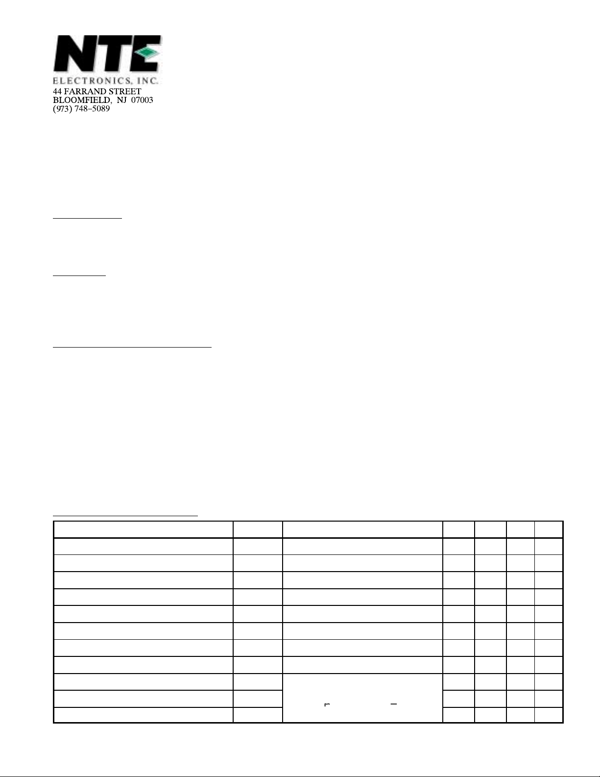
Schematic Diagram
B
C
E
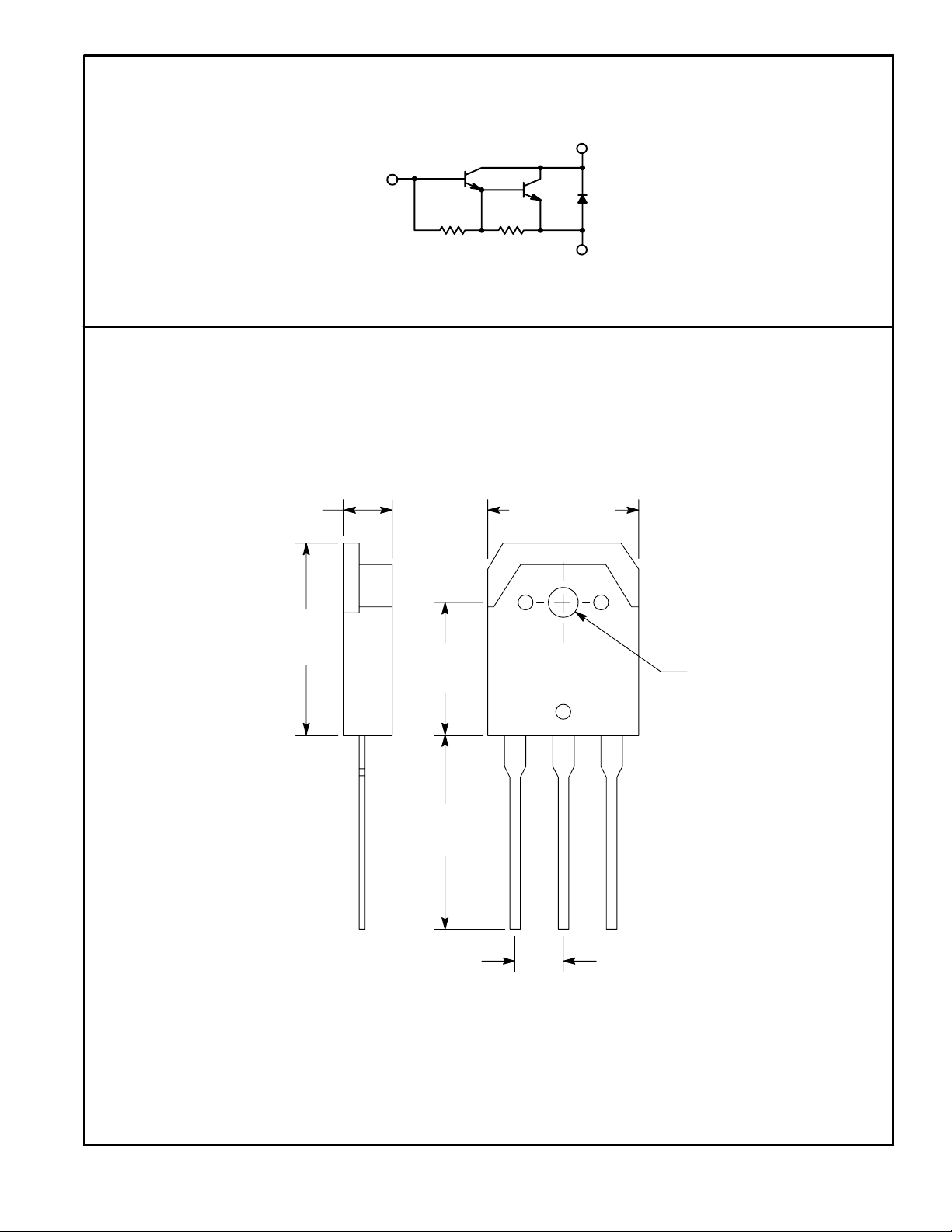
.190 (4.82)
.787
(20.0)
.591
(15.02)
.787
(20.0)
.615 (15.62)
C
.126
(3.22)
Dia
BCE
.215 (5.47)
 Loading...