

NTE NTE21128 Datasheet

NTE21128
Integrated Circuit
NMOS, 128K (16K x 8) UV EPROM
Description:
The NTE21128 is a 131,072 bit UV erasable and electrically programmable memory EPROM in a
28–Lead DIP type package organized as 16,384 words by 8 bits. The transparent lid allows the user
to expose the chip to ultraviolet light to erase the bit pattern. A new pattern can then be written to the
device by following the programming procedure.
Features:
D Access Time: 250ns
D Single 5V Supply Voltage
D Low Standby Current: 40mA Max
D TTL Compatible During Read and Program
D Fast Programming Algorithm
D Programming Voltage: 12V Typ
Absolute Maximum Ratings:
Supply Voltage, V
Program Supply, V
A9 Voltage, V
Input or Output Voltages, V
CC
PP
A9
IO
Ambient Operating Temperature, T
Temperature Under Bias, T
Storage Temperature Range, T
BIAS
stg
A
–0.6V to 6.25V. . . . . . . . . . . . . . . . . . . . . . . . . . . . . . . . . . . . . . . . . . . . . . . . . . . . . .
–0.6V to 14V. . . . . . . . . . . . . . . . . . . . . . . . . . . . . . . . . . . . . . . . . . . . . . . . . . . . . . .
–0.6V to 13.5V. . . . . . . . . . . . . . . . . . . . . . . . . . . . . . . . . . . . . . . . . . . . . . . . . . . . . . . . . .
–0.6V to 6.25V. . . . . . . . . . . . . . . . . . . . . . . . . . . . . . . . . . . . . . . . . . . . . .
0° to +70°C. . . . . . . . . . . . . . . . . . . . . . . . . . . . . . . . . . . . . . . . . . .
–10° to +80°C. . . . . . . . . . . . . . . . . . . . . . . . . . . . . . . . . . . . . . . . . . . . .
–65° to +125°C. . . . . . . . . . . . . . . . . . . . . . . . . . . . . . . . . . . . . . . . . .
Note 1. Except for the rating “Operating Temperature Range”, stresses above those listed in the
table “Absolute Maximum Ratings” may cause permanent damage to the device. These are
stress ratings only and operation of the device at these or any other conditions above those
indicated in the Operating sections of this specification is not implied. Exposure to Absolute
Maximum Rating conditions for extended periods may affect device reliability.
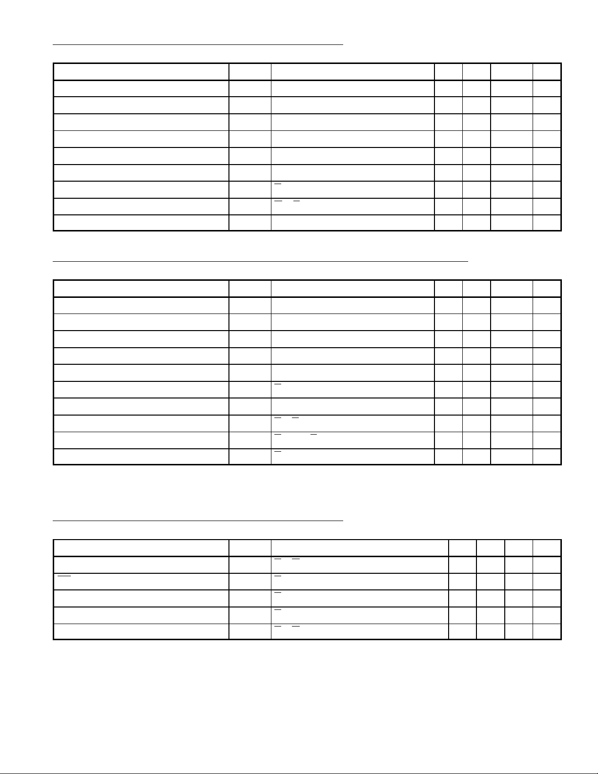
DC Characteristics (Read Mode and Standby Mode):
(TA = 0° to + 70°C, VCC = +5V ±5%, VPP = VCC)
Parameter Symbol Test Conditions Min Typ Max Unit
Output High Voltage V
Output Low Voltage V
Input High Voltage V
Input Low Voltage V
Output Leakage Current I
Input Leakage Current I
VCC Current (Standby) I
VCC Current (Active) I
VPP Current I
OHIOH
OLIOL
IH
IL
LO
LI
CC1
CC2
PP1
= –400µA 2.4 – – V
= 2.1mA – – 0.45 V
2.0 – VCC +1 V
–0.1 – 0.8 V
V
= 5.25V – – 10 µA
OUT
VIN = 5.25V – – 10 µA
E = V
IH
G = E = V
IL
– – 25 mA
– 60 100 mA
VPP = 5.25V – – 15 mA
DC Characteristics (Program, Program Verify, and Program Inhibit Modes):
(TA = +25°±5°C, VCC = +5V ±5% Note 2, VPP = +21V ±0.5V)
Parameter Symbol Test Conditions Min Typ Max Unit
Input High Voltage V
Input Low Voltage V
Input Leakage Current I
Output High Voltage V
Output Low Voltage V
VCC Current (Program Inhibit) I
VCC Current (Program Verify) I
VPP Current (Program) I
VPP Current (Program Verify) I
VPP Current (Program Inhibit) I
IH
IL
LI
OHIOH
OLIOL
CC1
CC2
PP2
PP3
PP4
VIN = VIL or V
= –400µA 2.4 – – V
IH
= 2.1mA – – 0.45 V
E = V
IH
E = P = V
E = VIL, P = V
E = V
IL
IH
IH
2.0 – VCC +1 V
–0.1 – 0.8 V
– – 10 µA
– – 25 mA
– – 100 mA
– – 30 mA
– – 15 mA
– – 15 mA
Note 2. VCC = 6V ±0.25V for high–speed programming.
AC Characteristics (Read Mode and Standby Mode):
(TA = 0° to + 70°C, VCC = +5V ±5%, VPP = VCC)
Parameter Symbol Test Conditions Min Typ Max Unit
Address to Output Delay t
CE to Output Delay t
Output Enable to Output Delay t
Output Enable High to Output Delay t
Address to Output Hold Time t
ACC
OE
OH
CE
DF
E = G = V
E = V
IL
E = V
IL
E = V
IL
E = G = V
IL
IL
Test Conditions:
Input Rise and Fall Times: 20ns
Input Pulse Levels: 0.45V to 2.4V
Timing Measurement Reference Levels:
Inputs: 0.8V and 2.0V
Outputs: 0.8V and 2.0V
– – 250 ns
– – 250 ns
– – 100 ns
0 – 85 ns
0 – – ns
 Loading...