


NTE210 (NPN) & NTE211 (PNP)
Silicon Complementary Transistors
General Purpose Output & Driver
Description:
The NTE210 (NPN) and NTE211 (PNP) are silicon complementary transistors in a T O202 type package designed for general purpose, medium voltage, medium power amplifier and driver applications
such as series, shunt and switching regulators, and low and high frequency inverters and converters.
Features:
D TO202 Type Package: 2W Free Air Dissipation @ TA = +25°C
Absolute Maximum Ratings:
Collector–Emitter Voltage, V
Collector–Emitter Voltage, V
Emitter–Base Voltage, V
Collector Current, I
C
CEO
CES
EBO
Continuous 1A. . . . . . . . . . . . . . . . . . . . . . . . . . . . . . . . . . . . . . . . . . . . . . . . . . . . . . . . . . . . . . . . . . .
Peak (Note 1) 2A. . . . . . . . . . . . . . . . . . . . . . . . . . . . . . . . . . . . . . . . . . . . . . . . . . . . . . . . . . . . . . . . .
Total Power Dissipation (T
= +25°C, Note 2), P
A
D
Derate Above 25°C 13.3mW/°C. . . . . . . . . . . . . . . . . . . . . . . . . . . . . . . . . . . . . . . . . . . . . . . . . . . .
Total Power Dissipation (T
= +25°C), P
C
D
Derate Above 25°C 50mW/°C. . . . . . . . . . . . . . . . . . . . . . . . . . . . . . . . . . . . . . . . . . . . . . . . . . . . . .
Operating Junction Temperature Range, T
Storage Temperature Range, T
stg
J
Lead Temperature (During Soldering, 1/16” from case, 10sec), T
Maximum Thermal Resistance, Junction–to–Ambient, R
Maximum Thermal Resistance, Junction–to–Case, R
thJA
thJC
–55° to +150°C. . . . . . . . . . . . . . . . . . . . . . . . . . . . . . . . . .
–55° to +150°C. . . . . . . . . . . . . . . . . . . . . . . . . . . . . . . . . . . . . . . . . .
L
75V. . . . . . . . . . . . . . . . . . . . . . . . . . . . . . . . . . . . . . . . . . . . . . . . . . . . . .
90V. . . . . . . . . . . . . . . . . . . . . . . . . . . . . . . . . . . . . . . . . . . . . . . . . . . . . .
5V. . . . . . . . . . . . . . . . . . . . . . . . . . . . . . . . . . . . . . . . . . . . . . . . . . . . . . . . . .
1.67W. . . . . . . . . . . . . . . . . . . . . . . . . . . . . . . . . . . . .
6.25W. . . . . . . . . . . . . . . . . . . . . . . . . . . . . . . . . . . . . . . . . . .
+260°C. . . . . . . . . . . . . . . . . . . . .
75°C/W. . . . . . . . . . . . . . . . . . . . . . . . .
20°C/W. . . . . . . . . . . . . . . . . . . . . . . . . . . .
Note 1. Pulse Test: Pulse Width ≤ 300µs.
Note 2. The actual power dissipation capability of the TO202 type package is 2W @ T
Electrical Characteristics:
Parameter Symbol Test Conditions Min Typ Max Unit
OFF Characteristics
Collector–Emitter Breakdown Voltage V
Collector Cutoff Current I
Emitter Cutoff Current I
(TA = +25°C unless otherwise specified)
(BR)CEOIC
CES
EBO
= 10mA, IB = 0 75 – – V
VCE = 90V – – 100 nA
VEB = 5V – – 100 nA
= +25°C.
A
Electrical Characteristics (Cont’d): (TA = +25°C unless otherwise specified)
Parameter Symbol Test Conditions Min Typ Max Unit
ON Characteristics (Note 3)
DC Current Gain h
Collector–Emitter Saturation Voltage V
Base–Emitter Saturation Voltage V
Dynamic Characteristics
Current–Gain Bandwidth Product f
Collector–Base Capacitance
NTE210
NTE211 – – 18 pF
FE
CE(sat)IC
BE(sat)IC
C
IC = 100mA, VCE = 2V 120 – 360
IC = 1A, VCE = 2V 10 – –
= 500mA, IB = 50mA – – 1.0 V
= 500mA, IB = 50mA – – 1.5 V
IC = 20mA, VCE = 10V, f = 20MHz 75 – 375 MHz
T
cb
VCB = 20V, IE = 0, f = 1MHz – – 12 pF
Note 3. Pulse Test: Pulse Width ≤ 300µs, Duty Cycle ≤ 2%.
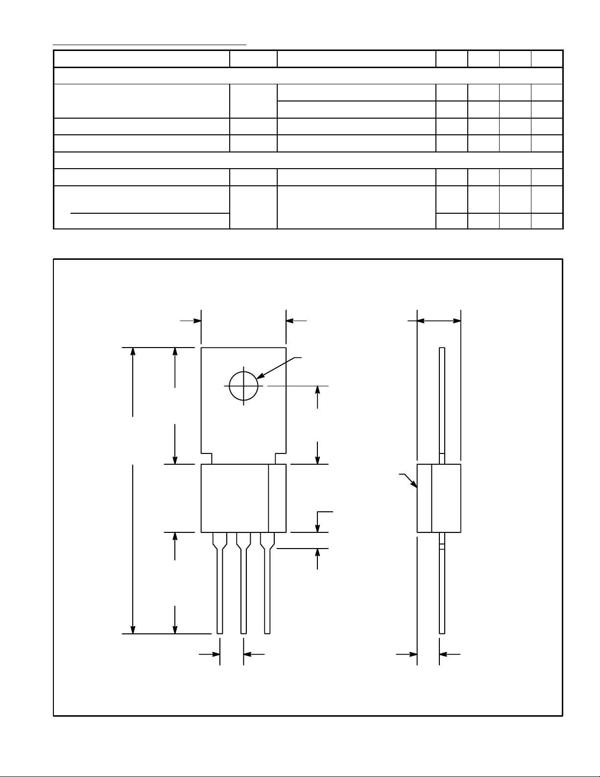
.180 (4.57).380 (9.56)
C
.132 (3.35) Dia
.500
(12.7)
1.200
.325
(9.52)
(30.48)
Ref
.070 (1.78) x 45°
.300
(7.62)
.400
(10.16)
Min
EBC
.100 (2.54) .100 (2.54)
Chamf
.050 (1.27)
 Loading...