

NTE NTE2090 Datasheet
NTE2090
Integrated Circuit
7–Channel Transistor Array
Description:
The NTE2090 is an integrated circuit in a 16–Lead DIP type package comprised of six NPN low saturation drivers. All units feature integral clamp diodes for switching inductive loads and protective
diodes for protection against a negative input voltage.
Features:
D Low Saturation Outputs:
V
CE(sat)
D Output Rating:
20V/150mA
D Output Clamp Diodes
D CMOS and PMOS Compatable Inputs
D Input Protection Diodes
Absolute Maximum Ratings: (TA = +25°C unless otherwise specified)
Supply Voltage, V
Output Sustaining Voltage, V
Output Current, I
Input Voltage, V
Input Current, I
Clamp Diode Reverse Voltage, V
Clamp Diode Forward Current, I
GND Pin Current, I
Power Dissipation, P
Operating Temperature Range, T
Storage Temperature Range, T
= 0.6V Max @ I
CC
OUT
IN
IN
GND
D
CE(sus)
R
F
opr
stg
= 120mA
OUT
–0.5V to +20V. . . . . . . . . . . . . . . . . . . . . . . . . . . . . . . . . . . . . . . . . . . . . . . . . . . . . . .
–0.5V to VCC +0.5V. . . . . . . . . . . . . . . . . . . . . . . . . . . . . . . . . . . . .
150mA. . . . . . . . . . . . . . . . . . . . . . . . . . . . . . . . . . . . . . . . . . . . . . . . . . . . . . . . . . . . .
–37V to +20V. . . . . . . . . . . . . . . . . . . . . . . . . . . . . . . . . . . . . . . . . . . . . . . . . . . . . . . . .
1.5mA. . . . . . . . . . . . . . . . . . . . . . . . . . . . . . . . . . . . . . . . . . . . . . . . . . . . . . . . . . . . . . . . .
20V. . . . . . . . . . . . . . . . . . . . . . . . . . . . . . . . . . . . . . . . . . . . . . . . . . . .
120mA. . . . . . . . . . . . . . . . . . . . . . . . . . . . . . . . . . . . . . . . . . . . . . . . . .
800mA. . . . . . . . . . . . . . . . . . . . . . . . . . . . . . . . . . . . . . . . . . . . . . . . . . . . . . . . . . .
1W. . . . . . . . . . . . . . . . . . . . . . . . . . . . . . . . . . . . . . . . . . . . . . . . . . . . . . . . . . . . . .
–40° to +85°C. . . . . . . . . . . . . . . . . . . . . . . . . . . . . . . . . . . . . . . . .
–55° to +150°C. . . . . . . . . . . . . . . . . . . . . . . . . . . . . . . . . . . . . . . . . .
Recommended Operating Conditions: (TA = –40° to +85°C unless otherwise specified)
Parameter Symbol Test Conditions Min Typ Max Unit
Supply Voltage V
Output Current I
Input Voltage V
Clamp Diode Reverse Voltage V
Clamp Diode Forward Voltage I
Power Dissipation P
OUT
CC
TPW = 25ms, DF = 10% 7 Circuits 0 – 100 mA
IN
R
F
D
4.75 – 18 V
0 – 120 mA
–35 – V
– – 18 V
– – 120 mA
– – 0.36 W
CC
V
Electrical Characteristics: (TA = +25°C unless otherwise specified)
Parameter Symbol Test Conditions Min Typ Max Unit
Output Leakage Current I
Output Saturation Voltage V
CE(sat)VCC
DC Forward Current Transfer Ratio h
Input Current
I
IN(ON)
Output ON
Output OFF I
IN(OFF)VIN
Clamp Diode Forward Voltage V
Supply Current
I
CC(ON)VCC
Output ON
Output OFF I
CC(OFF)VCC
Turn–On Delay t
Turn–Off Delay t
CEX
VCC = 18V, V
= 5V, IIN = 0.2mA, I
VCC = 5V, V
FE
VIN = 5V, I
OUT
VIN = 15V, I
= –35V – – –10 µA
IF = 120mA – 1.25 1.6 V
F
= VIN = 5V – 4 6
VCC = VIN = 15V – 14 22
= 18V, VIN = 0V – – 10 µA
ON
OFF
VCC = 18V, RL = 150Ω, CL = 15pF
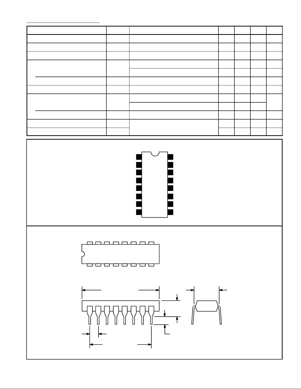
Pin Connection Diagram
1
I
1
2
I
2
3
I
3
4
I
4
5
I
5
6
I
6
7
I
7
GND
8
= 18V, TA = +75°C – – 100 µA
OUT
= 120mA – 0.45 0.6 V
OUT
OUT
= 2V, I
= 120mA 1000 – –
OUT
= 120mA – 0.16 0.23 mA
= 120mA – 0.66 0.94 mA
OUT
– 0.1 – µs
– 0.8 – µs
16
C
1
15
C
2
14
C
3
13
C
4
12
C
5
11
C
6
10
C
7
9
V
CC
mA/
Gate
16
1
9
8
.870 (22.0) Max .260 (6.6)
Max
.200 (5.08)
Max
.100 (2.54)
.099 (2.5) Min
.700 (17.78)
 Loading...