

NTE2088
Integrated Circuit
4–Segment Darlington Array, w/Pre–Driver Stage
for use with PMOS and 12V CMOS
Description:
The N TE2088 i s a H igh v oltage, hi gh c urrent D arlington a rray i n a 1 6–Lead DIP t ype package desi gned
as an i nterface b etween l ow–level l ogic a nd a v ariety o f p eripheral l oads s uch a s r elays, s olenoids, D C
and stepper motors, multiplexed LED and incandescent displays, heaters, and similar loads to 480
Watts (1.5A per output, 80V, 26% duty cycle).
This device has a minimum output breakdown of 50V and a minimum V
100mA, or a minimum output breakdown of 80V and a minimum V
CE(sus)
CE(sus)
of 50V.
of 35V measured at
A copper–alloy lead frame provides maximum power dissipation using standard cooling methods.
This lead configuration facilitates attachment of external heat sinks for increased power dissipation
with standard IC sockets and printed wiring boards.
Features:
D TTL, DTL, PMOS, CMOS Compatible Inputs
D Transient–Protected Outputs
D Loads to 480 Watts
D Heat Sink Contact Tabs on Quad Arrays
Absolute Maximum Ratings: (TA = +25°C unless otherwise specified)
Output Voltage, V
Output Sustaining Voltage, V
Output Current , I
80V. . . . . . . . . . . . . . . . . . . . . . . . . . . . . . . . . . . . . . . . . . . . . . . . . . . . . . . . . . . . . .
CEX
CE(sus)
1.75A. . . . . . . . . . . . . . . . . . . . . . . . . . . . . . . . . . . . . . . . . . . . . . . . . . . . . . . . . . . . .
OUT
50V. . . . . . . . . . . . . . . . . . . . . . . . . . . . . . . . . . . . . . . . . . . . . . . . . .
Input Voltage, VIN 30V. . . . . . . . . . . . . . . . . . . . . . . . . . . . . . . . . . . . . . . . . . . . . . . . . . . . . . . . . . . . . . . . . .
Input Current (Note 1), IB 25mA. . . . . . . . . . . . . . . . . . . . . . . . . . . . . . . . . . . . . . . . . . . . . . . . . . . . . . . . .
Supply Voltage, VS 20V. . . . . . . . . . . . . . . . . . . . . . . . . . . . . . . . . . . . . . . . . . . . . . . . . . . . . . . . . . . . . . . . .
Operating Temperature Range, TA –20° to +85°C. . . . . . . . . . . . . . . . . . . . . . . . . . . . . . . . . . . . . . . . . .
Storage Temperature Range, TS –55° to –150°C. . . . . . . . . . . . . . . . . . . . . . . . . . . . . . . . . . . . . . . . . . .
Note 1. Input current may be limited by maximum allowable input voltage.
Electrical Characteristics: (TA = +25°C unless otherwise specified)
Parameter Symbol Test Conditions Min Typ Max Unit
Output Leakage Current I
Output Sustaining Voltage V
CEX
CE(sus)IC
VCE = 80V – – 100 µA
VCE = 80V, TA = +70°C – – 500 µA
= 100mA, VIN = –400mV 50 – – V
Electrical Characteristics (Cont’d): (TA = +25°C unless otherwise specified)
Parameter Symbol Test Conditions Min Typ Max Unit
Collector–Emitter Saturation Voltage V
Input Current I
Input Voltage V
CE(sat)IC
IN(ON)
IN(ON)VCE
Supply Current I
Turn–On Delay t
Turn–Off Delay t
PLH
PHL
Clamp Diode Leakage Current I
Clamp Diode Forward Voltage V
= 500mA, VIN = 5V – – 1.1 V
IC = 750mA, VIN = 5V – – 1.2 V
IC = 1A, VIN = 5V – – 1.3 V
IC = 1.25A, VIN = 5V – – 1.4 V
IC = 1.5A, VIN = 5V – – 1.5 V
VIN = 5V – – 400 µA
VIN = 12V – – 1250 µA
= 2V, IC = 1.5A – – 5 V
IC = 500mA, VIN = 5V – – 4.5 mA
S
0.5 EIN to 0.5 E
0.5 EIN to 0.5 E
VR = 80V – – 50 µA
R
OUT
, IC = 1.25A – – 1.5 µs
OUT
– – 1.0 µs
VR = 80V, TA = +70°C – – 100 µA
IF = 1A – – 1.75 V
F
IF = 1.5A – – 2.0 V
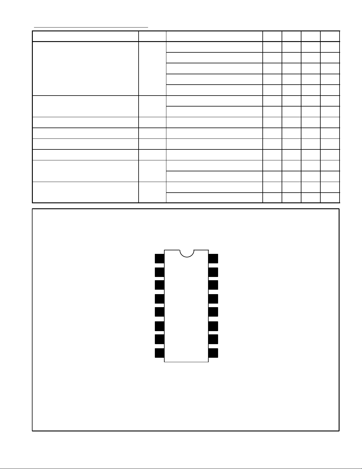
Pin Connection Diagram
K 1
C
2
B
3
4GND
GND
N.C.
5
6B
7
8
C
16
C
B
15
14
V
S
13
GND
12 GND
B
11
10 C
9
K
 Loading...