


NTE2087
Integrated Circuit
4–Stage Darlington Array
w
/Pre–Drive Stage for TTL
Description:
The NTE2087 is a H i gh – Voltage, High–Current Darlington Array designed to interface low–level logic
to a variety of peripheral loads such as relays, solenoids, d–c and stepper motors, multiplexed LED
and incandescent displays, heaters, and similar loads to 480 watts (1.5 A per output, 80V , 26% duty
cycle).
This device is specified with a minimum output breakdown of 50 volts and V
CE(sus)
minimum of 35
volts measured at 100mA and an output current specification of 1.5A (saturated).
A Quad driver Type, the NTE2087 is intended for use with TTL, low–speed TTL, and 5V MOS logic.
This device incorporates predriver stages and is most suitable for applications requiring high gain (low
input current loading).
Features:
D TTL, DTL, PMOS, CMOS Compatible Inputs
D Transient Protected Outputs
D Handle Loads to 480 Watts
D Plastic Dual In–Line Package with Heat Sink Contact Tabs
Absolute Maximum Ratings: (TA = +25°C for any one driver unless otherwise specified)
Output Voltage, V
Minimum Output Sustaining Voltage, V
Output Current, I
Input Voltage (Note 1), V
Input Current (Note 2), I
Supply Voltage, V
CEX
CE(sus)
OUT
IN
B
S
Operating Ambient Temperature Range, T
Storage Temperature Range, T
stg
opr
–20° to +85°C. . . . . . . . . . . . . . . . . . . . . . . . . . . . . . . . .
–55° to +150°C. . . . . . . . . . . . . . . . . . . . . . . . . . . . . . . . . . . . . . . . .
80V. . . . . . . . . . . . . . . . . . . . . . . . . . . . . . . . . . . . . . . . . . . . . . . . . . . . . . . . . . . . . . .
50V. . . . . . . . . . . . . . . . . . . . . . . . . . . . . . . . . . . . . . . . . .
1.75A. . . . . . . . . . . . . . . . . . . . . . . . . . . . . . . . . . . . . . . . . . . . . . . . . . . . . . . . . . . . . .
15V. . . . . . . . . . . . . . . . . . . . . . . . . . . . . . . . . . . . . . . . . . . . . . . . . . . . . . . . . .
25mA. . . . . . . . . . . . . . . . . . . . . . . . . . . . . . . . . . . . . . . . . . . . . . . . . . . . . . . . . .
10V. . . . . . . . . . . . . . . . . . . . . . . . . . . . . . . . . . . . . . . . . . . . . . . . . . . . . . . . . . . . . . . . .
Note 1. Input Voltage is with reference to ground
Note 2. Input Current may be limited by maximum allowable input voltage.
Electrical Characteristics: (TA = +25°C, VS = 5V unless otherwise specified)
Parameter Symbol Test Conditions Min Typ Max Unit
Output Leakage Current I
Collector–Emitter Saturation Voltage V
Input Current I
Input Voltage V
CEX
CE(sat)IC
IN(ON)VIN
IN(ON)VCE
Supply Current I
Turn–On Delay t
Turn–Off Delay t
Clamp Diode Leakage Current I
Clamp Diode Forward Voltage V
S
PLH
PHL
R
F
VCE = 80V – – 100 µA
VCE = 80V, TA = +70°C – – 500 µA
= 500mA, VIN = 2.75V – – 1.1 V
IC = 750mA, VIN = 2.75V – – 1.2 V
IC = 1.0A, VIN = 2.75V – – 1.3 V
IC = 1.25A, VIN = 2.75V – – 1.4 V
IC = 1.5A, VIN = 2.75V – – 1.5 V
= 2.75V – – 550 µA
VIN = 3.75V – – 1000 µA
= 2V, IC = 1.5A – – 2.75 V
IC = 500mA, VIN = 2.75V – – 6.0 mA
0.5Ein to 0.5E
0.5Ein to 0.5E
out
, IC = 1.25A – – 1.5 µs
out
– – 1.0 µs
VR = 80V – – 50 µA
VR = 80V, TA = +70°C – – 100 µA
IF = 1.0A – – 1.75 V
IF = 1.5A – – 2.0 V
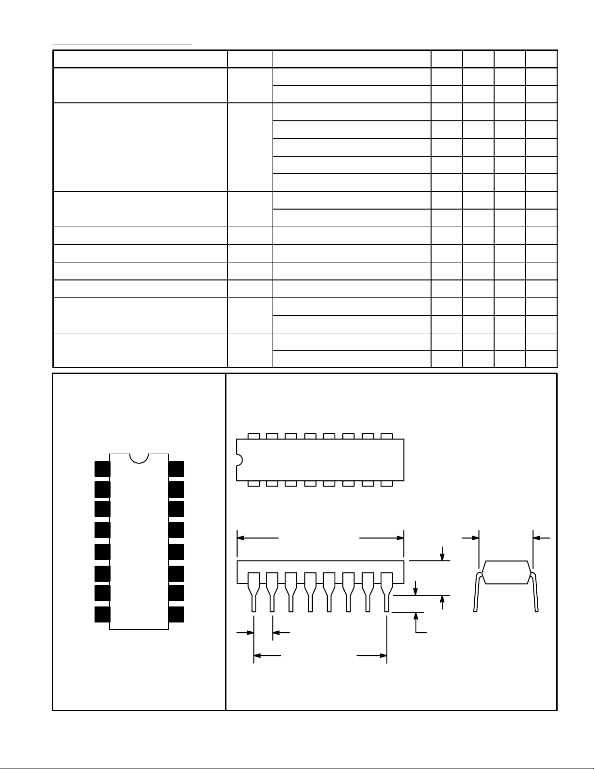
Pin Connection Diagram
1
K
2
C
B
3
GND
GND
N.C.
4
5
6B
7
C
8
16
15
14
13
12
11
10
9
C
B
V
S
GND
GND
B
C
K
16 9
18
.870 (22.0) Max .260 (6.6)
Max
.200 (5.08)
Max
.100 (2.54)
.700 (17.78)
.099 (2.5) Min
 Loading...