

NTE2080
Integrated Circuit
7–Stage Driver Array
Features:
D Low Output Saturation Voltage
D Protective Diodes Guard Against Negative Inputs
D Spark Killer Diodes Accommodate L–Loads
D Eqipped with a Strobe Terminal to Cut Off Outputs
D With 7 Units, it is Ideal for 14–Digit Printers
Applications:
D Driving Battery–Operated Compact Printers
D Driving Various Relays
D Driving LED Lamps and Other Display Elements
D Interfacing with MOS or Bipolar Logic IC
Absolute Maximum Ratings
Output Supply Voltage, V
Input Supply Voltage, V
IN(1)
Strobe Supply Voltage, V
Maximum Power Supply Voltage, V
Output Inflow Current (Per Unit, at V
Instantaneous Output Inflow Current (Per Unit, Note 1), I
Spark–Killer Diode Forward Current (Per Unit, Note 1), I
GND–Pin Outflow Current (Note 1), I
V
Instantaneous Outflow Current (Note 1), I
CC
Allowable Power Dissipation (T
Operating Ambient Temperature Range, T
Storage Ambient Temperature Range, T
Note 1. Pulse Width < 35ms at V
Allowable Operating Conditions
Supply Voltage, V
CC
Input H–Level Voltage (I
Input L–Level Voltage (I
ST Input H–Level (V
ST Input L–Level (V
OUT
= 20V, I
IN
= 20V, I
IN
: (TA = +25°C unless otherwise specified)
OUT
IN(2)
max –0.3V to +9V. . . . . . . . . . . . . . . . . . . . . . . . . . . . . . . . . . . . .
CC
), I
IH
OUT
op
F(s)
9
ccp
= +55°C), PDmax 500mW. . . . . . . . . . . . . . . . . . . . . . . . . . . . . . . . .
A
opg
stg
, Duty Cycle = 10%.
IH
: (TA = +25°C unless otherwise specified)
= 100mA), V
OUT
= 100µA), V
OUT
OUT
= 100µA), V
= 100µA), V
IH
IL
SH
SL
Load Inductance (“L” With Spark–Killer Diodes Employed), L
–0.3V to +11V. . . . . . . . . . . . . . . . . . . . . . . . . . . . . . . . . . . . . . . . . . . . . . .
–35V to +20V. . . . . . . . . . . . . . . . . . . . . . . . . . . . . . . . . . . . . . . . . . . . . . . . .
0V to +10V. . . . . . . . . . . . . . . . . . . . . . . . . . . . . . . . . . . . . . . . . . . . . . . . .
100mA. . . . . . . . . . . . . . . . . . . . . . . . . . . . . . . . . . . . . . . .
150mA. . . . . . . . . . . . . . . . . . . . . . . . . . .
150mA. . . . . . . . . . . . . . . . . . . . . . . . . . .
–1050mA. . . . . . . . . . . . . . . . . . . . . . . . . . . . . . . . . . . . . . . . . . . .
–1050mA. . . . . . . . . . . . . . . . . . . . . . . . . . . . . . . . . .
–20° to +80°C. . . . . . . . . . . . . . . . . . . . . . . . . . . . . . . . .
–40° to +125°C. . . . . . . . . . . . . . . . . . . . . . . . . . . . . . . . . . .
3.5V to 9V. . . . . . . . . . . . . . . . . . . . . . . . . . . . . . . . . . . . . . . . . . . . . . . . . . . . . . . . . .
8V to 20V. . . . . . . . . . . . . . . . . . . . . . . . . . . . . . . . . . . . . .
–30V to +1V. . . . . . . . . . . . . . . . . . . . . . . . . . . . . . . . . . . . .
2V to 8V. . . . . . . . . . . . . . . . . . . . . . . . . . . . . . . . . .
0V to 0.3V. . . . . . . . . . . . . . . . . . . . . . . . . . . . . . . . .
L
≤ 100mH. . . . . . . . . . . . . . . . . . . . . . .
Electrical Characteristics: (TA = +25°C unless otherwise specified)
Parameter Symbol Test Conditions Min Typ Max Unit
Output Voltage V
Output Sustaining Voltage V
Output Leakage Current I
Input Current I
Input Leakage Current I
Spark–Killer Diode Leakage Current I
Spark–Killer Diode Forward Voltage V
Power Supply Current Strobe HI I
leak(s)VOUT
OUT
O(sus)VIN
Leak
IDL
VIN = 8V, VCC = 6V, I
IIN = 300µA, VCC = 6V, I
IIN = 300µA, VCC = 8V, I
= Open, t < 10µs, I
VIN = 1V, VCC = 9V – – 100 µA
off
VIN = 20V, I
In
VIN = –30V –10 – – µA
= 0, VCC = 8V – – 30 µA
= 150mA – – 1.7 V
F(s)IF(s)
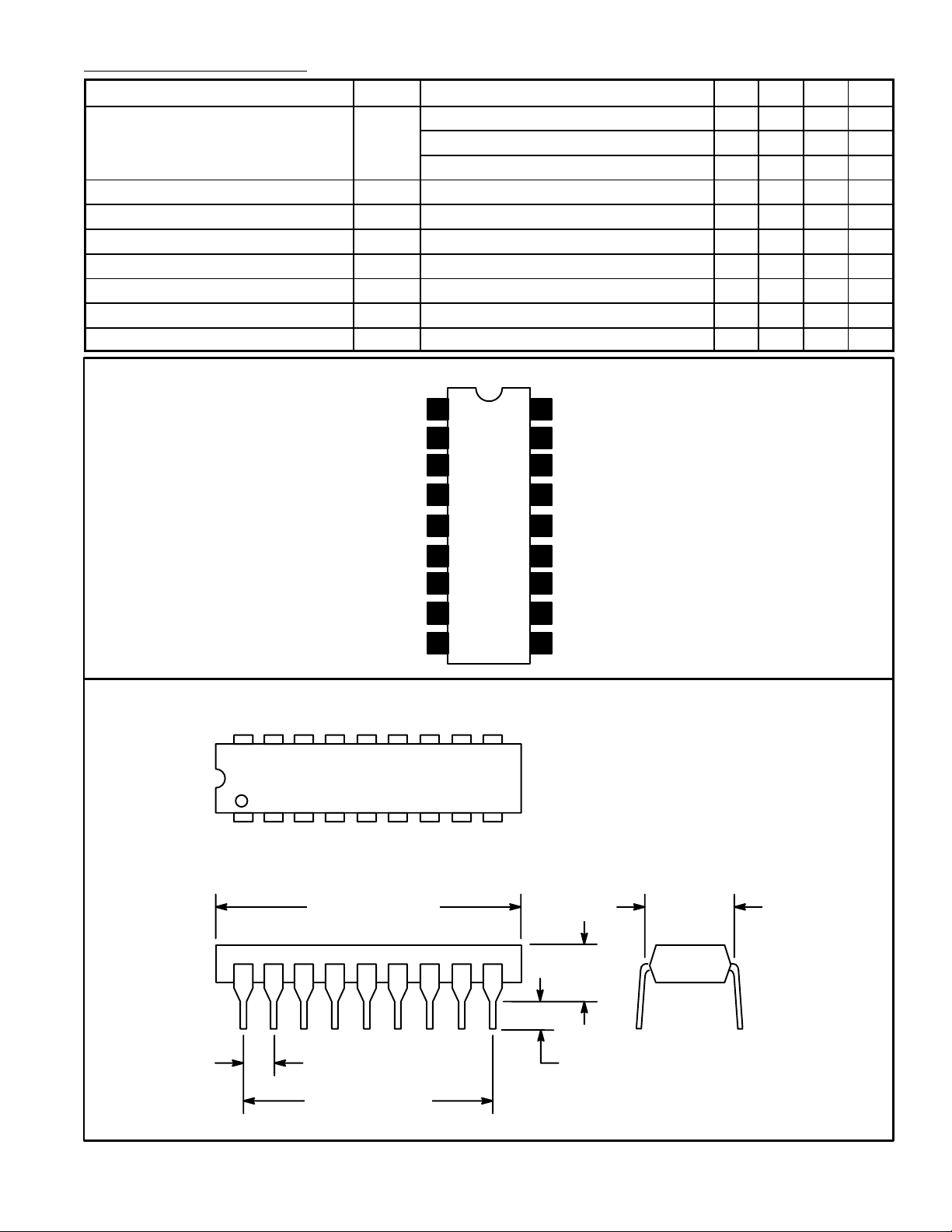
Pin Connection Diagram
VIN = 20V, VCC = 9V – – 18 mA
= 0 – – 1.8 mA
OUT
= 100mA – – 0.25 V
OUT
= 100mA – – 0.25 V
OUT
= 150mA – – 0.5 V
OUT
= 150mA 11 – – V
OUT
Test
Input 1
Input 2
Input 3
GND
1
2
3
4
5Input 4
6Input 5
7Input 6
8Input 7
9 10
ST
18
Output 1
17
16
Output 2
15
Output 3
14 Output 4
13 Output 5
Output 6
12
Output 7
11
V
CC
18 10
19
.952 (24.2)
.100 (2.54)
.800 (20.32)
.300
(7.62)
.143
(3.65)
.131 (3.35)
 Loading...