

NTE NTE2072 Datasheet
NTE2072
Integrated Circuit
Transistor Array w/Clamp Diode and Strobe
Description:
The NTE2072 is a 6–Channel sink driver consisting of 12 NPN transistors to form high current gain
driver pairs.
Each input has a diode and 1.6kΩ resistor in series to allow a negative voltage input. All inputs can
be controlled simultaneously by a strobe input at Pin1.
The power supply of the predrivers is connected to Pin16. All emitters and the substrate are connected together to Pin8. Each output has an integral diode for inductive load transient suppression
and the cathodes of the diodes are connected to Pin9.
The outputs are capable of sinking 320mA and will withstand 20V in the OFF state.
Absolute Maximum Ratings: (TA = –20° to +75°C unless otherwise specified)
Supply Voltage, VCC 10V. . . . . . . . . . . . . . . . . . . . . . . . . . . . . . . . . . . . . . . . . . . . . . . . . . . . . . . . . . . . . . .
Output Sustaining Voltage (Transistor OFF), V
CEO
Collector Current (Transistor ON), IC 320mA. . . . . . . . . . . . . . . . . . . . . . . . . . . . . . . . . . . . . . . . . . . . . .
Input Voltage, VI –25V to +20V. . . . . . . . . . . . . . . . . . . . . . . . . . . . . . . . . . . . . . . . . . . . . . . . . . . . . . . . . .
Strobe Input Voltage, V
Clamp Diode Reverse Voltage, V
Clamp Diode Forward Current, I
20V. . . . . . . . . . . . . . . . . . . . . . . . . . . . . . . . . . . . . . . . . . . . . . . . . . . . . . . .
I(STB)
20V. . . . . . . . . . . . . . . . . . . . . . . . . . . . . . . . . . . . . . . . . . . . . . . . .
R(D)
320mA. . . . . . . . . . . . . . . . . . . . . . . . . . . . . . . . . . . . . . . . . . . . . . .
F(D)
Power Dissipation (TA = +25°C), Pd 1.47W. . . . . . . . . . . . . . . . . . . . . . . . . . . . . . . . . . . . . . . . . . . . . . . .
Operating Ambient Temperature Range, T
Storage Temperature Range, T
–55° to +125°C. . . . . . . . . . . . . . . . . . . . . . . . . . . . . . . . . . . . . . . . . .
stg
–20° to +75°C. . . . . . . . . . . . . . . . . . . . . . . . . . . . . . . . .
opr
–0.5V to +20V. . . . . . . . . . . . . . . . . . . . . . . . . . . .
Recommended Operational Conditions: (TA = –20° to +75°C, unless otherwise specified)
Parameter Symbol Test Conditions Min Typ Max Unit
Supply Voltage V
Output Voltage V
Collector Current
(Per Channel)
CC
I
O
C
Percent Duty Cycle
less than 25%, VCC = 8.5V
Percent Duty Cycle
3 – 8 V
0 – 20 V
0 – 300
0 – 150
less than 85%, VCC = 6.5V
“H” Input Voltage V
IH
IC = 300mA 3.2 – 18 V
mA
Recommended Operational Conditions (Cont’d): (TA = –20° to +75°C, unless otherwise specified)
Parameter Symbol Test Conditions Min Typ Max Unit
“L” Input Voltage V
“H” Input Voltage
V
IH(STB)
IL
IC = 50µA 0 – 0.7 V
2.4 – 18 V
(Strobe Input)
“L” Input Voltage
V
IL(STB)
0 – 0.2 V
(Strobe Input)
Electrical Charactersistics: (TA = –20° to +75°C, unless otherwise specified)
Parameter Symbol Test Conditions Min Typ Max Unit
Output Sustaining Voltage V
Output Saturation Voltage V
(BR)CEOVCC
CE(sat)
= 8V, VI = 3.2V,
V
I(STB)
= 0.2V, I
VI = 3V,
V
I(STB)
= 2.4V
= 100µA
CEO
VCC = 6.5V,
IC = 250mA
VCC = 3.0V,
20 – – V
– 0.5 0.55
– 0.3 0.5
IC = 120mA
Input Current I
Input Leakage Current I
I
R
VCC = 8V, VI = 3.2V,
V
I(STB)
= 2.4V
– – 1.4 mA
VCC = 8V, VI =–25V – – –20 µA
V
Strobe Input Current I
Strobe Input Leakage Current I
t(STB)
R(STS)
Clamp Diode Forward Voltage V
Clamp Diode Reverse Voltage V
Supply Current I
DC Forward Current Gain h
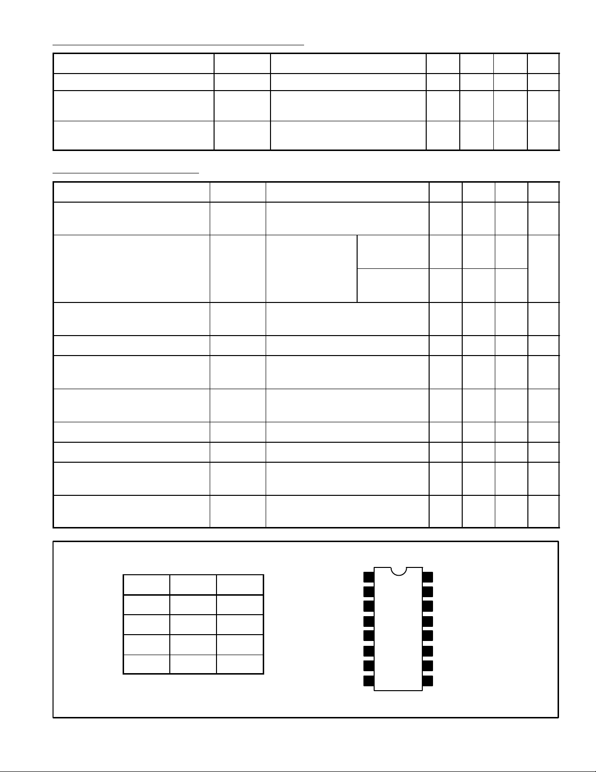
Functional Table Pin Connection Diagram
IN STB OUT
L L H
H L H
L H H
H H L
F(D)
R(D)
CC
FE
VCC = 8V, VI = 3.2V (all input),
V
I(STB)
= 0.2V
VCC = 8V, VI = 0V,
V
I
F(D)
I
R(D)
= 20V
I(STB)
= 320mA – 1.4 2.4 V
= 100µA 20 40 – V
VCC = 8V, VI = 3.2V (all input),
V
I(STS)
= 2.4V
VCE = 4V, VCC = 5.5V,
– –7.9 – mA
– – 20 µA
– 120 200 mA
1000 3000 – –
IC = 300mA, TA = +25°C
STB 1
Input 1
Input 2
Input 4
Input 6
GND
2
3
4Input 3
5
6Input 5
7
8
V
16
CC
Output 1
15
Output 2
14
13
Output 3
12 Output 4
Output 5
11
10 Output 6
Common
9
 Loading...