

NTE NTE2061, NTE2060 Datasheet

NTE2060 & NTE2061
Integrated Circuit
PMOS LSI Alarm Clock Circuit
Applications:
D Alarm Clock
D Clock Radio
D Timer for Home Appliances
D Display of Elapsed Time
Functions:
D Real Time Display
D Alarm With Snooze Function
D Sleep Timer (59 Minutes Max)
Features:
D Single Chip P–Channel ED MOS LSI
D Direct Drive Capable:
LED (5mA or More, Red LED)
Fluorescent Display Tube (Light–Up Voltage 16V or Less)
D Wide Operating Voltage Range: –8V to –16V
D Capable of 50Hz or 60Hz Reference Frequency
D Two Selections of Display Mode:
AM/PM 12–Hour
24–Hour
D 24–Hour Alarm Function
D Repeatable Snooze Function
D Presettable 59–Minute Down Counter (Sleep Timer)
D SNOOZE Pin can be used to Set the Sleep Timer with One Touch
D Clock Input Noise Eliminator
D Power Failure Indicating Function (All Digits Flashing):
12H Display Mode → AM or OUTPUT of LSI
24H Display Mode → AM, PM or b & c OUTPUT of LSI
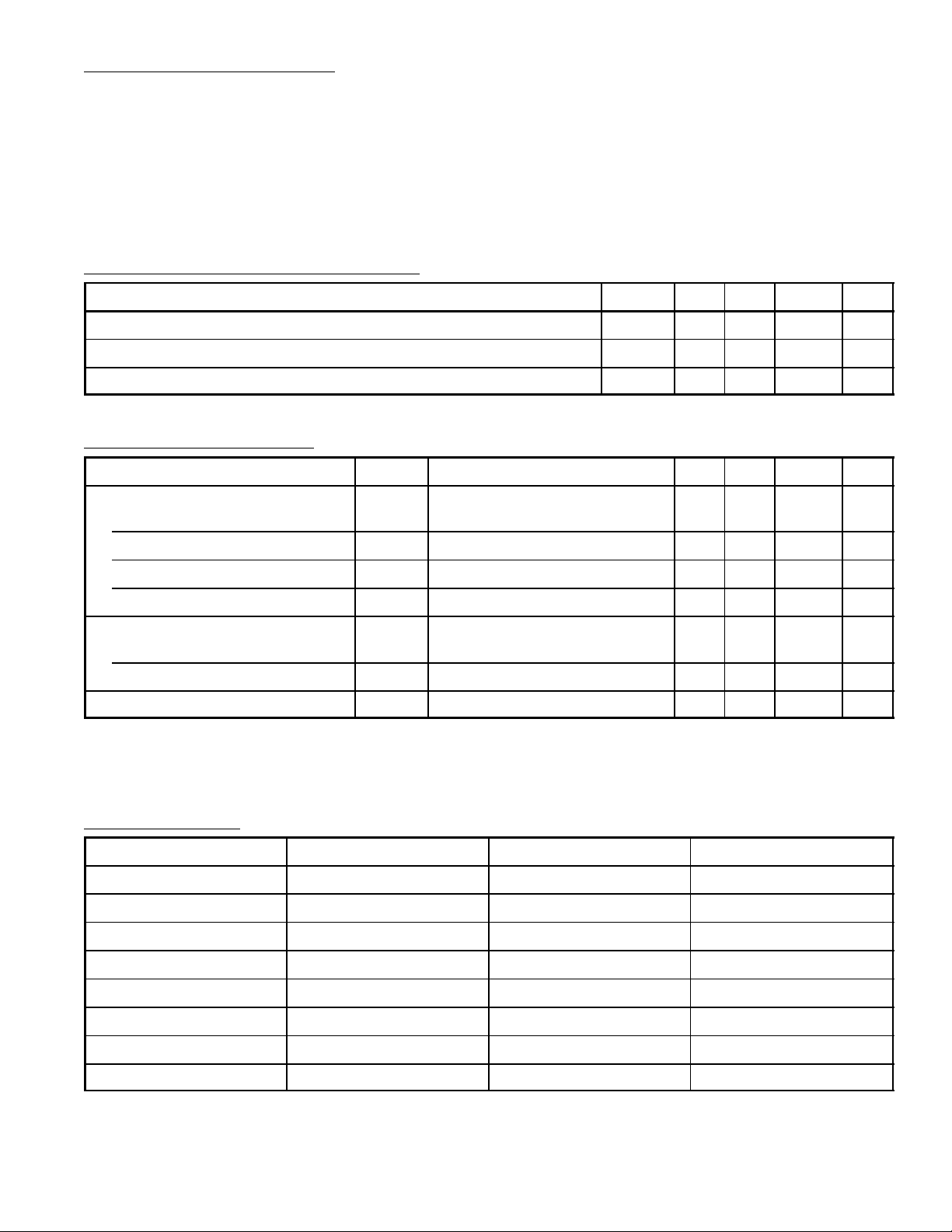
Absolute Maximum Ratings: (TA = +25°C, VSS = 0V unless otherwise specified)
Maximum Supply Voltage, VDDmax –18 to +0.3V. . . . . . . . . . . . . . . . . . . . . . . . . . . . . . . . . . . . . . . . . . .
Input Voltage, V
IN
Output Voltage (Output Pin OFF), V
OUT
VDD –0.3 to +0.3V. . . . . . . . . . . . . . . . . . . . . . . . . . . . . . . . . . . . . . . . . . . . . . . . . . . . .
VDD –0.3 to +0.3V. . . . . . . . . . . . . . . . . . . . . . . . . . . . . . . . . .
Allowable Power Dissipation (TA = +70°C), PDmax 900mW. . . . . . . . . . . . . . . . . . . . . . . . . . . . . . . . . .
Operating Temperature Range, T
Storage Temperature Range, T
stg
opr
–30° to +70°C. . . . . . . . . . . . . . . . . . . . . . . . . . . . . . . . . . . . . . . . .
–55° to +125°C. . . . . . . . . . . . . . . . . . . . . . . . . . . . . . . . . . . . . . . . . .
Recommended Operating Conditions: (TA = +25°C, VSS = 0V unless otherwise specified)
Parameter Symbol Min Typ Max Unit
Supply Voltage V
Input “H” Level Voltage V
Input “L” Level Voltage V
DD
IH
IL
–16 –12 –8 V
–1 – 0 V
V
DD
– VDD +2 V
Electrical Characteristics: (TA = +25°C, VSS = 0V, VDD = 12V ±2V unless otherwise specified)
Parameter Symbol Test Conditions Min Typ Max Unit
Output “H” Level Current
ALARM OUT, SLEEP OUT
b & c, a & d I
1Hz I
All Other Outputs I
I
OH (1)
OH (2)
OH (3)
OH (4)
VOH = VSS – 2V 0.5 – – mA
VOH = VSS – 2.5V 10 – – mA
VOH = VSS – 2.5V 13 – – mA
VOH = VSS – 2.5V 5 – Note 1 mA
Output Leakage Current
ALARM OUT, SLEEP OUT
All Other Outputs I
Current Dissipation I
I
OL (1)
OL (2)
DD
VOL = V
DD
– – 5 µA
VOL = VDD + 1.8V – – 50 µA
VDD = –12V – 3 – mA
Note 1. 11mA Max is allowed in the range where the power dissipation is 900mW and 1.2W at
TA = +70°C and +25°C respectively.
Function Table A:
Alarm Display Input Seconds Display Input Sleep Display Input Display Mode
L L L Real Time Display
H L L Alarm Display
L H L Seconds Display
H H L Alarm Display
L L H Sleep Display
H L H Sleep Display
L H H Sleep Display
H H H Sleep Display
Note 2. “H”: Input Pin ––– VSS Level
“L”: Input Pin ––– VDD Level (or Open)
 Loading...