


NTE2057
Integrated Circuit
Dual 16–Bit Digital–to–Analog Converter
for CD and DAT Players
Description:
The NTE2057 is a monolithic integrated dual 16–bit digital –to–analog converter (DAC) in a 28–Lead
DIP type package designed for use in Hi–Fi digital audio equipment such as compact disc players,
digital tape, or cassette recorders.
Features:
D Selectable Input Format: Offset Binary or Two’s Complement
D Internal Timing and Control Circuit
D TTL–Compatible Digital Inputs
D High Maximum Input Bit Rate and Fast Settling Time
D 6Mbits/s Data Rate
D Low Linearity Error (1/2 LSB typ)
D Fast Settling (1µs typ)
Applications:
D Compact Disc Players
D Digital Audio Tape, and Cassette Recorders and Players
D Waveform Generation
Absolute Maximum Ratings:
Supply Voltage Range, V
Pin28 (VDD) +7V. . . . . . . . . . . . . . . . . . . . . . . . . . . . . . . . . . . . . . . . . . . . . . . . . . . . . . . . . . . . . . . . .
Pin26 (V
Pin15 (V
Junction Temperature Range, T
Operating Ambient Temperature Range, T
Storage Temperature Range, T
Electrostatic Handling (Note 1), VES –1000 to +1000V. . . . . . . . . . . . . . . . . . . . . . . . . . . . . . . . . . . . . .
Note 1. Discharging a 250pF capacitor through a 1kΩ series resistor.
) –7V. . . . . . . . . . . . . . . . . . . . . . . . . . . . . . . . . . . . . . . . . . . . . . . . . . . . . . . . . . . . . . . .
DD1
) –17V. . . . . . . . . . . . . . . . . . . . . . . . . . . . . . . . . . . . . . . . . . . . . . . . . . . . . . . . . . . . . . .
DD2
DD
J
A
stg
–55° to +150°C. . . . . . . . . . . . . . . . . . . . . . . . . . . . . . . . . . . . . . . . . . .
–20° to +70°C. . . . . . . . . . . . . . . . . . . . . . . . . . . . . . . . . . .
–65° to +150°C. . . . . . . . . . . . . . . . . . . . . . . . . . . . . . . . . . . . . . . . . .
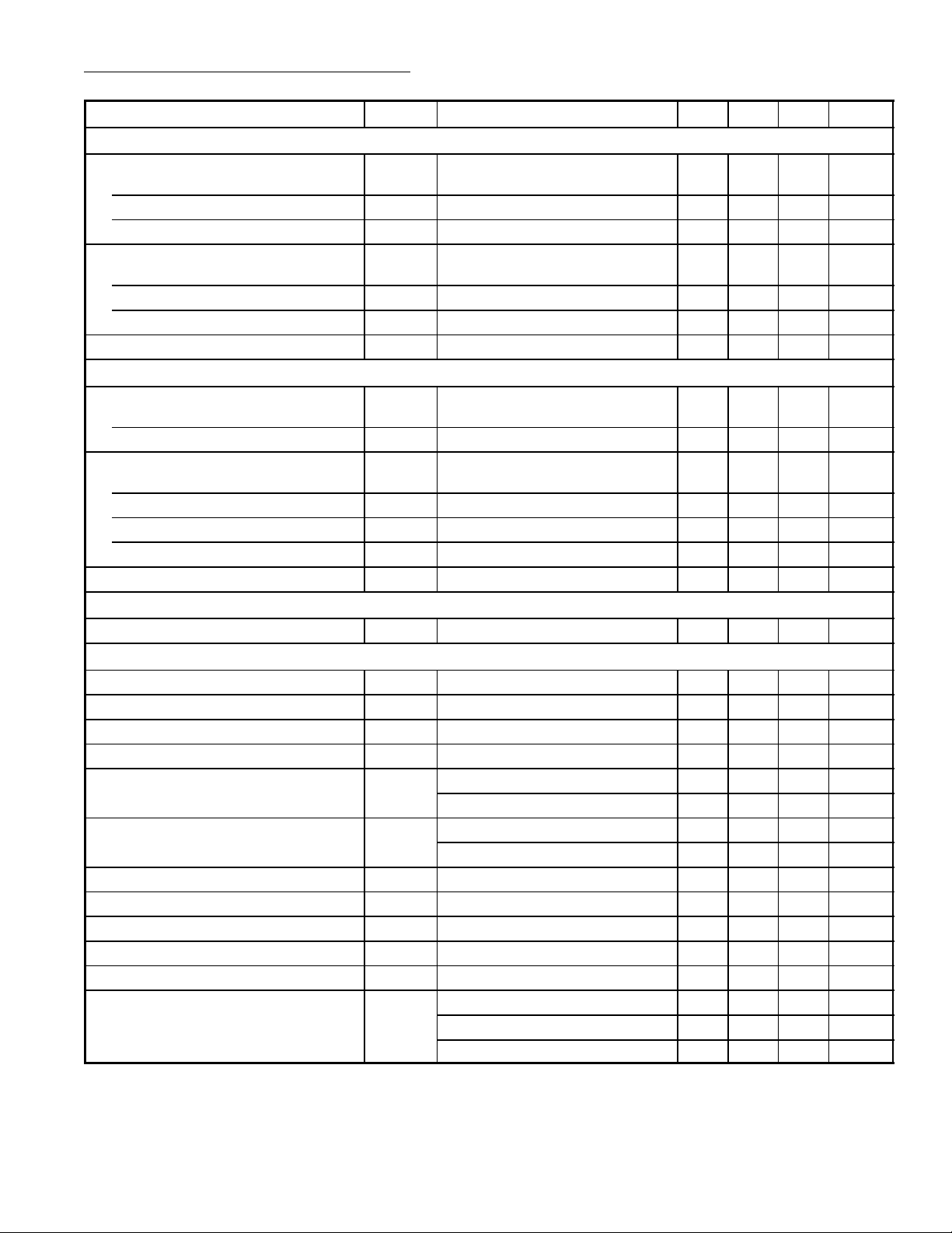
DC and AC Electrical Characteristics: (VDD = +5V, V
= –5V, V
DD1
= –15V, TA = +25°C
DD2
unless otherwise specified)
Parameter Symbol Test Conditions Min Typ Max Unit
Supply
Supply Voltage Range
Pin28 V
Pin26 –V
Pin15 –V
DD
DD1
DD2
Supply Currents
Pin28 I
Pin26 –I
Pin15 –I
DD
DD1
DD2
Resolution – 16 – bits
Inputs
Input Current (Pin3, Pin4)
Digital Inputs Low I
Digital Inputs High I
< 0.8V – – TBD mA
IL
> 2.0V – – TBD µA
IH
Input Frequency
At Clock Input (Pin4) f
At Clock Input (Pin2) f
At Data Inputs (Pin3, Pin4) f
At Word Select Input (Pin1) f
Input Capacitance of Digital Inputs C
SCK
BCK
DAT
WS
I
Oscillator
Oscillator Fr equency w/Internal Capacitor f
OSC
Analog Outputs (AOL, AOR)
Output Voltage Compliance V
Full–Scale Current I
Zero–Scale Current ±I
Full–Scale Temperature Coefficient TC
Linearity Error Integral E
FS
CC
ZS
TA = –20° to +70°C – ±200 – ppm/°C
FS
TA = +25°C – 0.5 – LSB
1
TA = –20° to +70°C – TBD – LSB
Linearity Error Differential E
D1
TA = +25°C – 0.5 1.0 LSB
TA = –20° to +70°C – TBD – LSB
Signal–to–Noise Ratio + THD S/N Note 2 90 95 – dB
Setting Time to ±1 LSB t
CS
Channel Separation T 80 TBD – dB
Unbalance Between Outputs ∆I
Time Delay Between Outputs t
FS
D
Power Supply Ripple Rejection (Note 3) RR VDD = +5V – TBD – dB
V
= –5V – TBD – dB
DD1
V
= –15V – TBD – dB
DD2
4.0 5.0 6.0 V
4.5 5.0 6.0 V
14.0 15.0 16.0 V
– 45 60 mA
– 45 75 mA
– 25 60 mA
– – 6 MHz
– – – MHz
– – – MHz
– – – kHz
– 12 – pF
150 200 250 kHz
TBD – TBD mV
3.4 4.0 4.6 mA
– TBD – nA
– 1 – µs
– 0.1 0.2 dB
– – 1 µs
Note 2. Signal–to–noise ratio + THD with 1kHz full–scale sine wave generated at a sampling rate
of 176.4kHz.
Note 3. V
RIPPLE
= 1% of supply voltage and f
RIPPLE
= 100Hz.
 Loading...