

NTE NTE2056 Datasheet

NTE2056
Integrated Circuit
8–Bit Multiplying Digital–to–Analog Converter
Description:
The NTE2056 is an 8–bit multiplying D–to–A converter in a 16–Lead DIP type package designed for
use where the output current is a linear product of an eight–bit digital word and an analog input voltage.
Features:
D Fast Setting Time: 300ns Typ
D Non–Inverting Digital Inputs are MTTL and CMOS Compatible
D Output Voltage Swing: +0.4V to –5.0V
D High–Speed Multipling Input: Slew Rate 4.0mA/µs
D Standard Supply Voltages: +5.0V and –5.0V to –15V
Applications:
D Tracking A–to–D Converters
D Successive Approximation A–to–D Converters
D 2 1/2 Digit Panel Meters and DVM’s
D Waveform Synthesis
D Sample and Hold
D Peak Detector
D Programmable Gain and Attenuation
D CRT Character Generation
D Audio Digitizing and Decoding
D Programmable Power Supplies
D Analog–Digital Multiplication
D Digital–Digital Multiplication
D Analog–Digital Division
D Digital Addition and Subtraction
D Speech Compression and Expansion
D Stepping Motor Drive
Absolute Maximum Ratings: (TA = +25°C unless otherwise specified)
Power Supply Voltage
V
CC
V
EE
Digital Input Voltage, V5 thru V
Applied Output Voltage, V
Reference Current, I
14
12
O
Reference Amplifier Inputs
V
. . . . . . . . . . . . . . . . . . . . . . . . . . . . . . . . . . . . . . . . . . . . . . . . . . . . . . . . . . . . . . . . . . . . . . . . .
14
V
. . . . . . . . . . . . . . . . . . . . . . . . . . . . . . . . . . . . . . . . . . . . . . . . . . . . . . . . . . . . . . . . . . . . . . . . .
15
Operating Temperature Range, T
Storage Temperature Range, T
A
stg
+5.5V. . . . . . . . . . . . . . . . . . . . . . . . . . . . . . . . . . . . . . . . . . . . . . . . . . . . . . . . . . . . . . . . . . . . . .
–16.5V. . . . . . . . . . . . . . . . . . . . . . . . . . . . . . . . . . . . . . . . . . . . . . . . . . . . . . . . . . . . . . . . . . . . . .
0 to +5.5V. . . . . . . . . . . . . . . . . . . . . . . . . . . . . . . . . . . . . . . . . . . . . . .
+0.5V, –5.2V. . . . . . . . . . . . . . . . . . . . . . . . . . . . . . . . . . . . . . . . . . . . . . . . . .
5mA. . . . . . . . . . . . . . . . . . . . . . . . . . . . . . . . . . . . . . . . . . . . . . . . . . . . . . . . . . . . .
V
CC
V
EE
0° to +75°C. . . . . . . . . . . . . . . . . . . . . . . . . . . . . . . . . . . . . . . . . . . . .
–65° to +150°C. . . . . . . . . . . . . . . . . . . . . . . . . . . . . . . . . . . . . . . . . .
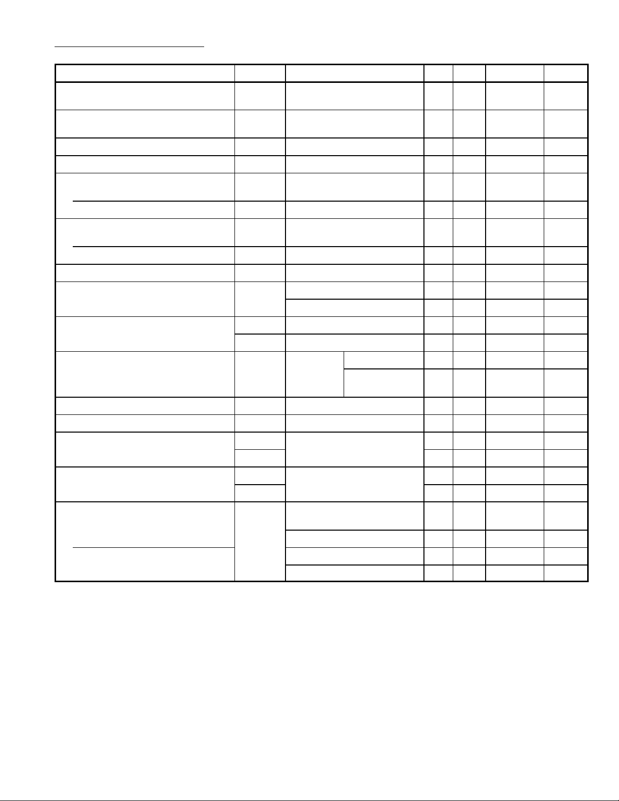
Electrical Characteristics: (TA = 0° to +75°C, VCC = +5V, VEE = –15V, V
inputs at high logic level, unless otherwise specified)
Parameter Symbol Test Conditions Min Typ Max Unit
Relative Accuracy
(Error relative to full scale IO)
E
Setting Time to within ±1/2 LSB
(Includes t
Propagation Delay Time t
PLH
)
t
PLH
Output Full Scale Current Drift TCI
Digital Input Logic Levels (MSB)
High Level, Logic “1”
V
Low Level, Logic “0” V
Digital Input Current (MSB)
High Level
I
Low Level I
Reference Input Bias Current (Pin15) I
Output Current Range I
OR
S
, t
IH
IL
15
r
PHLTA
O
IH
IL
Note 1
TA = +2 5°C, Note 2
– – ±0.78 %
– 300 – ns
= +2 5°C – 30 100 ns
– –20 – PPM/°C
2.0 – – V
– – 0.8 V
VIH = 5V
– 0 0.04 mA
VIL = 0.8V – –0.4 –0.8 mA
– –1.0 –5.0 µA
VEE = –5V 0 2.0 2.1 mA
VEE = –15V, TA = +2 5°C 0 2.0 4.2 mA
/R14 = 2mA, All digital
ref
Output Current I
I
O (min)
Output Voltage Compliance V
O
V
= 2.000V, R14 = 1000Ω 1.9 1.99 2.1 mA
ref
All bits low – 0 4.0 µA
O
Er ≤ 0.19%,
TA = +2 5°C
Pin1 Grounded – – –0.55, +0.4 V
Pin1 Open,
– – –5.0, +0.4 V
VEE below –10V
Reference Current Slew Rate SR I
ref
– 4.0 – mA/µs
Output Current Power Supply Sensitivity PSRR(–) – 0.5 2.7 µA/V
Power Supply Current I
Power Supply Voltage Range V
Power Dissipation
All bits low
V
CC
I
EE
CCR
EER
P
All bits low – +13.5 +22.0 mA
– –7.5 –13.0 mA
TA = +2 5°C +4.5 +5.0 +5.5 V
–4.5 –15.0 –16.5 V
D
VEE = –5V
– 105 170 mW
VEE = –15V – 190 305 mW
All bits high VEE = –5V – 90 – mW
VEE = –15V – 160 – mW
Note 1. All current switches are tested to guarantee at least 50% of rated output current.
Note 2. All bits switched.
 Loading...