

NTE NTE2054 Datasheet

NTE2054
Integrated Circuit
A/D Converter for 3–Digit Display
Description:
The NTE2054 is an I2L monolithic Analog to Digital converter in a 16–Lead DIP type package that
provides a 3–digit multiplexed BCD output. This device, when used with an NTE2032 BCD–to–
Seven–Segment Decoder/Driver and a minimum of external parts, implements a complete 3–digit
display.
Features:
D Dual–Slope A/D Conversion
D Multiplexed BCD Display
D Ultra–Stable Internal Band–Gap Voltage Reference
D Capable of Reading 99mV below GND with a Single Supply
D Differential Input
D Internal Timing – No External Clock Required
D Choice of Low–Speed (4Hz) or High–Speed (96Hz) Conversion Rate
D “Hold” Inhibits Conversion but Maintains Delay
Absolute Maximum Ratings:
DC Supply Voltage (between Pin7 and Pin14), V+ +7V. . . . . . . . . . . . . . . . . . . . . . . . . . . . . . . . . . . . . .
Input Voltage (Pin10 or Pin11 to GND), V
Device Dissipation (Up to TA = +55°C), P
I
D
750mW. . . . . . . . . . . . . . . . . . . . . . . . . . . . . . . . . . . . . . . . . .
Derate Linearly Above TA = +55°C 7.9mW/°C. . . . . . . . . . . . . . . . . . . . . . . . . . . . . . . . . . . . . . . .
Operating Temperature Range, T
Storage Temperature Range, T
Lead Temperature, T
L
stg
A
0° to +75°C. . . . . . . . . . . . . . . . . . . . . . . . . . . . . . . . . . . . . . . . . . . . .
–65° to +150°C. . . . . . . . . . . . . . . . . . . . . . . . . . . . . . . . . . . . . . . . . .
(During Soldering, 1/16 ±1/32 in. (1.59 ±0.79mm) from case for 10sec Max) +265°C. . . . . .
±15V. . . . . . . . . . . . . . . . . . . . . . . . . . . . . . . . . . . . . . . . . . . .
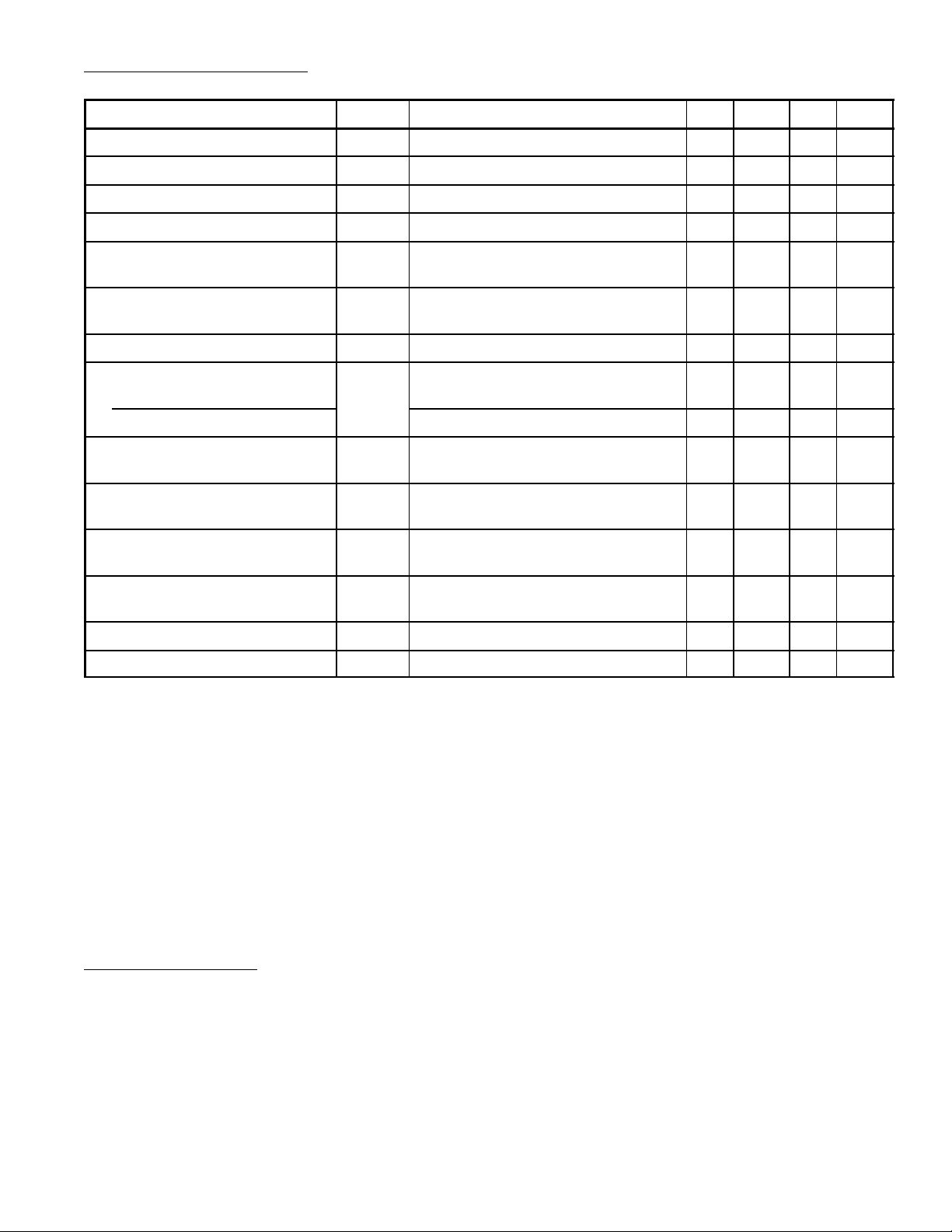
Electrical Characteristics:(TA = +25°C, V+ = 5V, Zero pot centered, gain pot = 2.4kΩ unless
otherwise specified)
Parameter Symbol Test Conditions Min Typ Max Unit
Operating Supply Voltage Range V+ 4.5 5.0 5.5 V
Supply Current I+ 100kΩ to V+ on Pin3, Pin4, Pin5 – – 17 mA
Input Impedance Z
Input Bias Current I
Unadjusted Zero Offset V11 –V10 = 0V,
Unadjusted Gain V11 –V10 = 900mV,
Linearity Note 1, Note 2 –1 – +1 Count
Conversion Rate
Slow Mode
Fast Mode Pin6 = 5V – 96 – Hz
Conversion Control Voltage
(Hold Mode) at Pin6
Common–Mode Input
Voltage Range
BCD Sink Current at
Pin1, Pin2, Pin15, and Pin16
Digit Select Sink Current at
Pin3, Pin4, and Pin5
Zero Temperature Coefficient VI = 0V, Zero Pot Centered – 10 – µV/°V
i
IB
V
ICR
Pin10 and Pin11 – –80 – nA
Read Decoded Output
Read Decoded Output
Pin6 = Open or GND – 4 – Hz
Note 3, Note 4 –0.2 – +0.2 V
V
≥ 0.5V, at Logic Zero State 0.4 1.6 – mA
BCD
V
Digit Select
= 4V at Logic Zero State 1.6 2.5 – mA
– 100 – MΩ
–12 – +12 mV
846 – 954 mV
0.8 1.2 1.6 V
Gain Temperature Coefficient VI = 900mV, Gain Pot = 2.4kΩ – 0.005 – %/°C
Note 1. Apply zero v o l t s a c r o s s V11 to V10. Adjust zero potentiometer to give 000mV reading. Apply
900mV to input and adjust gain potentiometer to give 900mV reading.
Note 2. Linearity is measured as a difference from a straight line drawn through zero and positive
full scale. Limits do not include ±0.5 count bit digitizing error.
Note 3. For applications where negative Pin10 is not operated at Pin7 potential, a return path of not
more than 100kΩ resistance must be provided for input bias currents.
Note 4. The common–mode input voltage above ground cannot exceed +0.2V if the full input signal
range of 999mV is required at Pin11. That is, Pin11 may not operate higher than 1.2V positive with respect to GND or 0.2V negative with respect to GND. If the maximum input signal
is less than 999mV, the common–mode input voltage may be raised accordingly.
Circuit Description:
The heart of the NTE2054 is the V/I converter and reference–current generator. The V/I converter
converts the input voltage applied between Pin10 and Pin11 to a current that charges the integrating
capacitor on Pin12 for a predetermined time interval. At the end of the charging interval, the V/I converter is disconnected from the integrated capacitor, and a band–gap reference constant–current
source of opposite polarity is connected. The number of clock counts that elapse before the charge
is restored to its original value is a direct measure of the signal induced current. The restoration is
sensed by the comparator , which in turn latches the counter. The count is then multiplexed to the BCD
outputs.
 Loading...