


NTE2053
Integrated Circuit
8–Bit MPU Compatible A/D Converter
Description:
The NT E2053 i s a C MOS 8–bi t s uccessive appr oximation Analog t o D igi tal converter i n a 2 0–Lead DIP
type p ackage w hich uses a d if ferential potentiometr ic l adder – s imilar t o t he 256R products. T his d evice
is d esigned t o a llow o perati on w i th the N SC800 a nd I NS8080A d erivative c ontrol b us, a nd T RI–STA TE
output latches d i rectly d rive t he d ata b us. These A/Ds a ppear l ike memory locations o r I /O p orts t o t he
microprocessor and no interfacing logic is needed.
A new differential analog voltage input allows increasing the common–mode rejection and offsetting
the analog zero input voltage value. In addition, the voltage reference input can be adjusted to allow
encoding any similar analog voltage span to the full 8 bits of resolution.
Features:
D Compatible With 8080 MPU Derivatives – No Interfacing Logic Needed – Access Time: 135ns
D Easy Interface to all Microprocessors, or Operates “Stand Alone”
D Differential Analog Voltage Inputs
D Logic Inputs and Outputs Meet Both MOS and TTL Voltage Level Specifications
D Works With 2.5V (NTE952) Voltage Reference
D On–Chip Clock Generator
D 0V to 5V Analog Input Voltage Range with Single 5V Supply
D No Zero Adjust Required
D Operates Ratiometrically or with 5V, 2.5V, or Analog Span Adjusts Voltage Reference
R
Absolute Maximum Ratings: (Note 1, Note 2)
Supply Voltage (Note 3), V
CC
6.5V. . . . . . . . . . . . . . . . . . . . . . . . . . . . . . . . . . . . . . . . . . . . . . . . . . . . . . .
Voltage at Logic Control Inputs –0.3V to +18V. . . . . . . . . . . . . . . . . . . . . . . . . . . . . . . . . . . . . . . . . . . . . .
Voltage at All Other Inputs and Outputs –0.3V to VCC +0.3V. . . . . . . . . . . . . . . . . . . . . . . . . . . . . . . . .
Storage Temperature Range, T
Power Dissipation (TA = +25°C), P
stg
D
Lead Temperature (During Soldering, 10sec), T
L
–65° to +150°C. . . . . . . . . . . . . . . . . . . . . . . . . . . . . . . . . . . . . . . . . .
875mW. . . . . . . . . . . . . . . . . . . . . . . . . . . . . . . . . . . . . . . . . . . . . . .
+300°C. . . . . . . . . . . . . . . . . . . . . . . . . . . . . . . . . . . .
Recommended Operating Conditions: (Note 1, Note 2)
Operating Temperature Range, T
Supply Voltage Range, V
CC
A
0° to +70°C. . . . . . . . . . . . . . . . . . . . . . . . . . . . . . . . . . . . . . . . . . . . .
4.5V to 6.3V. . . . . . . . . . . . . . . . . . . . . . . . . . . . . . . . . . . . . . . . . . . . . . . . .
Note 1. Absolute Maximum Ratings are those values beyond which the life of the device may be im-
paired.
Note 2. All voltage are measured with respect to GND, unless otherwise specified. The separate
A GND point should always be wired to the D GND.
Note 3. A zener d i ode exists, internal ly, f rom VCC to G N D a nd h as a typical breakdown v ol tage o f 7V.
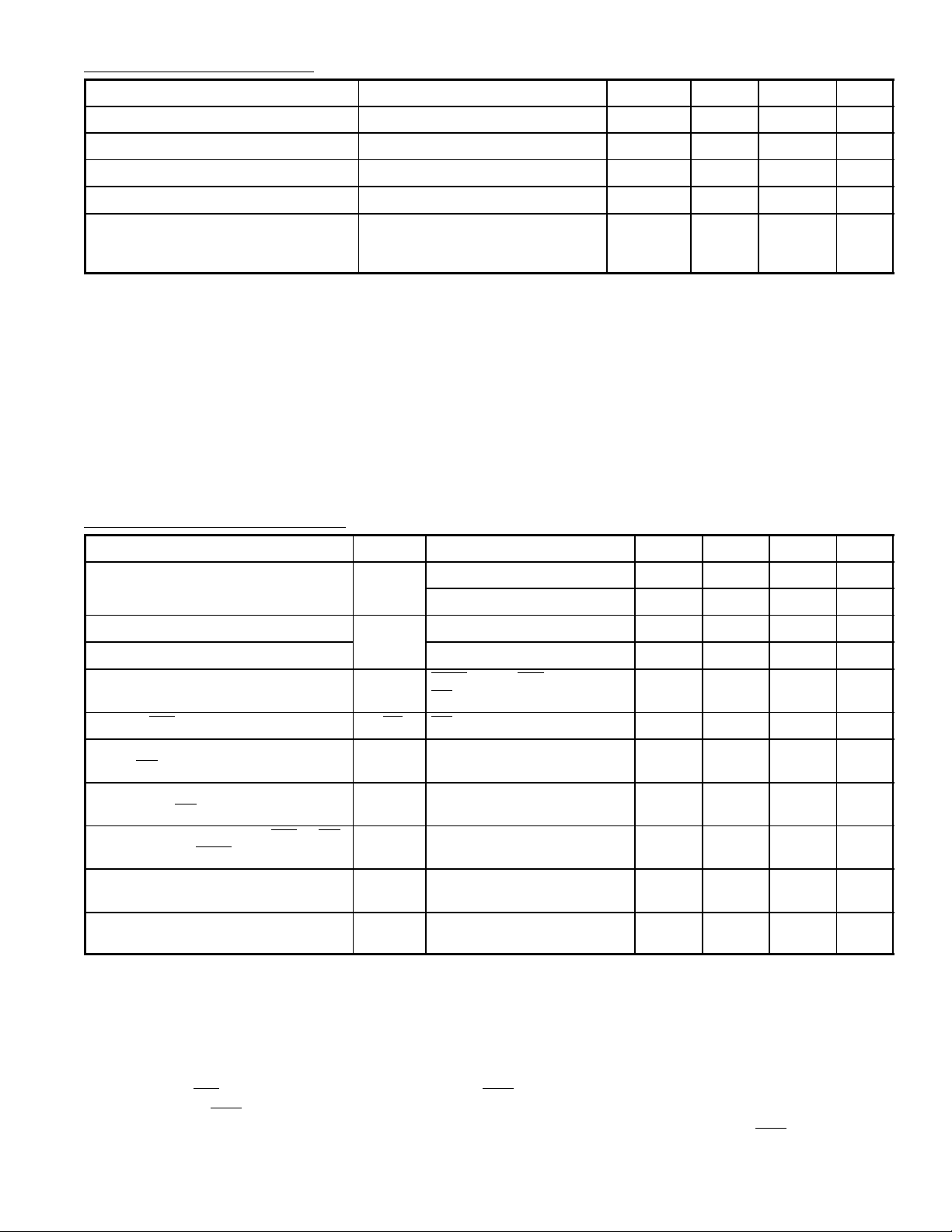
Electrical Characteristics: (VCC = 5V, TA = 0° to +70°C, f
Parameter Test Conditions Min Typ Max Unit
= 640kHz unless otherwise specified)
CLK
Total Unadjusted Error (Note 4) V
V
/2 Input Resistance 2.5 8.0 – kΩ
REF
Analog Input Voltage Range V(+) or V(–), Note 5 GND–0.05 – VCC+0.05 V
DC Common–Mode Error Over Analog Input Voltage Range – ±1/
Power Supply Sensitivity VCC = 5V ±10% Over Allowed
/2 = 2.500V – – ±1/
REF
±1/
VIN(+) and VIN(–) Voltage Range,
Note 5
16
16
±1/
±1/
2
8
8
LSB
LSB
LSB
Note 4. The NTE2053 A/D does not require a zero adjust.
Note 5. For VIN(–) ≥ VIN(+) the digital output code will be 0000 0000. Two on–chip diodes are tied
to each analog input which will forward conduct for analog input voltages one diode drop belwo GND or one diode drop greater than the VCC supply . Be careful, during testing at low V
CC
levels (4.5V), as high level analog inputs (5V) can cause this input diode to conduct – especially at elevated temperatures, and cause errors for analog inputs near full–scale. The spec
allows 50mV forward bias of either diode. This means that as long as the analog VIN does
not exceed the supply voltage by more than 50mV, the output code will be correct. To
achieve an absolute 0V to 5V input voltage range will therefore require a minimum supply
voltage of 4.950V over temperature variations, initial tolerance, and loading.
AC Electrical Characteristics: (VCC = 5V, TA = +25°C unless otherwise specified)
Parameter Symbol Test Conditions Min Typ Max Unit
Conversion Time T
Clock Frequency f
Clock Duty Cycle Note 6 40 – 60 %
Conversion Rate in Free–Running
Mode
Width of WR Input (Start Pulse Width) t
Access Time (Delay from Falling Edge
of RD to Output Data Valid)
TRI–STATE Control (Delay from Rising
Edge of RD to Hi–Z State)
Delay from Falling Edge of WR or RD
to Reset of INTR
Input Capacitance of Logic
Control Inputs
TRI–STATE Output Capacitance
(Data Buffers)
CLK
CR INTR tied to WR with
W(WR)L
t
ACC
t1H, t
tWI, t
C
C
OUT
Note 6. Accuracy is guaranteed at f
f
C
0HCL
RI
IN
CLK
= 640kHz, Note 7 103 – 114 µs
CLK
Note 6, Note 7 66 – 73 1/f
VCC = 5V, Note 6 100 640 1460 kHz
– – 8770 conv/s
CS = 0V, f
CS = 0, Note 8 100 – – ns
CL = 100pF – 135 200 ns
= 10pF, RL = 10k – 125 200 ns
= 640kHz
CLK
– 300 450 ns
– 5 7.5 pF
– 5 7.5 pF
= 640kHz. At higher clock frequencies accuracy can de-
CLK
grade. For lower clock frequencies, the duty cycle limits can be extended so long as the minimum clock high time interval or minimum clock low time interval is no less than 275ns.
Note 7. With an asynchronous start pulse, up to 8 clock periods may be required before the internal
clock phases are proper to start the conversion process. The start request is internally
latched.
Note 8. The CS input is assumed to bracket the WR strobe input and therefore timing is dependent
on the WR pulse width. An arbitrary wide pulse width will hold the converter on a reset mode
and the start of conversion is initiated by the low to high transition of the WR pulse.
 Loading...