

NTE NTE2033 Datasheet
NTE2033
Integrated Circuit
Non–Inverting Transistor Array, Low Input Active
Description:
The NTE2033 is a non–inverting transistor array, which is comprised of four NPN darlington output stages and PNP input stages. This device is low level input active driver and is suitable for
operation with TTL, 5V C–MOS and 5V Microprocessor which have sink current output drivers.
Features:
D Output Current: 1.5A Max.
D High Sustaining Voltage: 50V Min.
D Low Level Active Inputs
D TTL and C–MOS Compatible Inputs
D Standard Supply Voltage
D Two VCC Terminals V
Absolute Maximum Ratings: (TA = +25°C unless otherwise specified)
Supply Voltage, V
CC
Output Sustaining Voltage, V
Output Current, I
Input Current, I
OUT
IN
Input Voltage, VIN –0.5 to +30V. . . . . . . . . . . . . . . . . . . . . . . . . . . . . . . . . . . . . . . . . . . . . . . . . . . . . . . . . .
Clamp Diode Reverse Voltage, V
Clamp Diode Forward Current, I
Common Terminal Current, I
GND Terminal Current, I
Power Dissipation, P
D
Operating Temperature Range, T
Storage Temperature Range, T
CC1
GND
, V
CC2
CE(sus)
F
COM
stg
(Separated)
R
opr
–0.5 to 10V. . . . . . . . . . . . . . . . . . . . . . . . . . . . . . . . . . . . . . . . . . . . . . . . . . . . . . . . .
–0.5 to +50V. . . . . . . . . . . . . . . . . . . . . . . . . . . . . . . . . . . . . . . . . . .
1.5A. . . . . . . . . . . . . . . . . . . . . . . . . . . . . . . . . . . . . . . . . . . . . . . . . . . . . . . . . . . . . . .
–10mA. . . . . . . . . . . . . . . . . . . . . . . . . . . . . . . . . . . . . . . . . . . . . . . . . . . . . . . . . . . . . . . .
50V. . . . . . . . . . . . . . . . . . . . . . . . . . . . . . . . . . . . . . . . . . . . . . . . . . . .
1.5A. . . . . . . . . . . . . . . . . . . . . . . . . . . . . . . . . . . . . . . . . . . . . . . . . . . .
3.0A. . . . . . . . . . . . . . . . . . . . . . . . . . . . . . . . . . . . . . . . . . . . . . . . . . . .
5.0A. . . . . . . . . . . . . . . . . . . . . . . . . . . . . . . . . . . . . . . . . . . . . . . . . . . . . . . .
2.7W. . . . . . . . . . . . . . . . . . . . . . . . . . . . . . . . . . . . . . . . . . . . . . . . . . . . . . . . . . . . .
–40° to +85°C. . . . . . . . . . . . . . . . . . . . . . . . . . . . . . . . . . . . . . . . .
–55° to +150°C. . . . . . . . . . . . . . . . . . . . . . . . . . . . . . . . . . . . . . . . . .
Recommended Operating Conditions: (TA = –40° to +85°C unless otherwise specified)
Parameter Symbol Test Conditions Min Typ Max Unit
Supply Voltage
Output Sustaining Voltage
Output Current
Input Voltage
Clamp Diode Reverse Voltage
Clamp Diode Forward Voltage
Power Dissipation
V
V
CE(sus)
I
OUT
V
V
V
P
CC
IN
R
F
D
4.5 – 5.5 V
0 – 50 V
0
0 – 25 V
0 – 50 µA
0 – 1.25 A
0 – 1.0 W
–
1.25 V
Electrical Characteristics: (TA = +25°C unless otherwise specified)
Parameter Symbol Test Conditions Min Typ Max Unit
“H” Level Input V oltage V
“C” Level Input V oltage V
“H” Level Input Current I
“L” Level Input Current I
Output Leak Current I
Collector–Emitter Saturation Voltage V
Clamp Diode Reverse Current I
Clamp Diode Forward Voltage V
Supply Current
Turn–ON Delay t
Turn–OFF Delay t
CE(sat)VCC
I
CC(ON)VCC
I
CC(OFF)VCC
VCC 1
GND/Heat Sink GND/Heat Sink
IH
IL
IH
VCC = 5.5V, VIN = 0.4V – –0.05 –0.36 mA
IL
V
CEX
R
F
ON
OFF
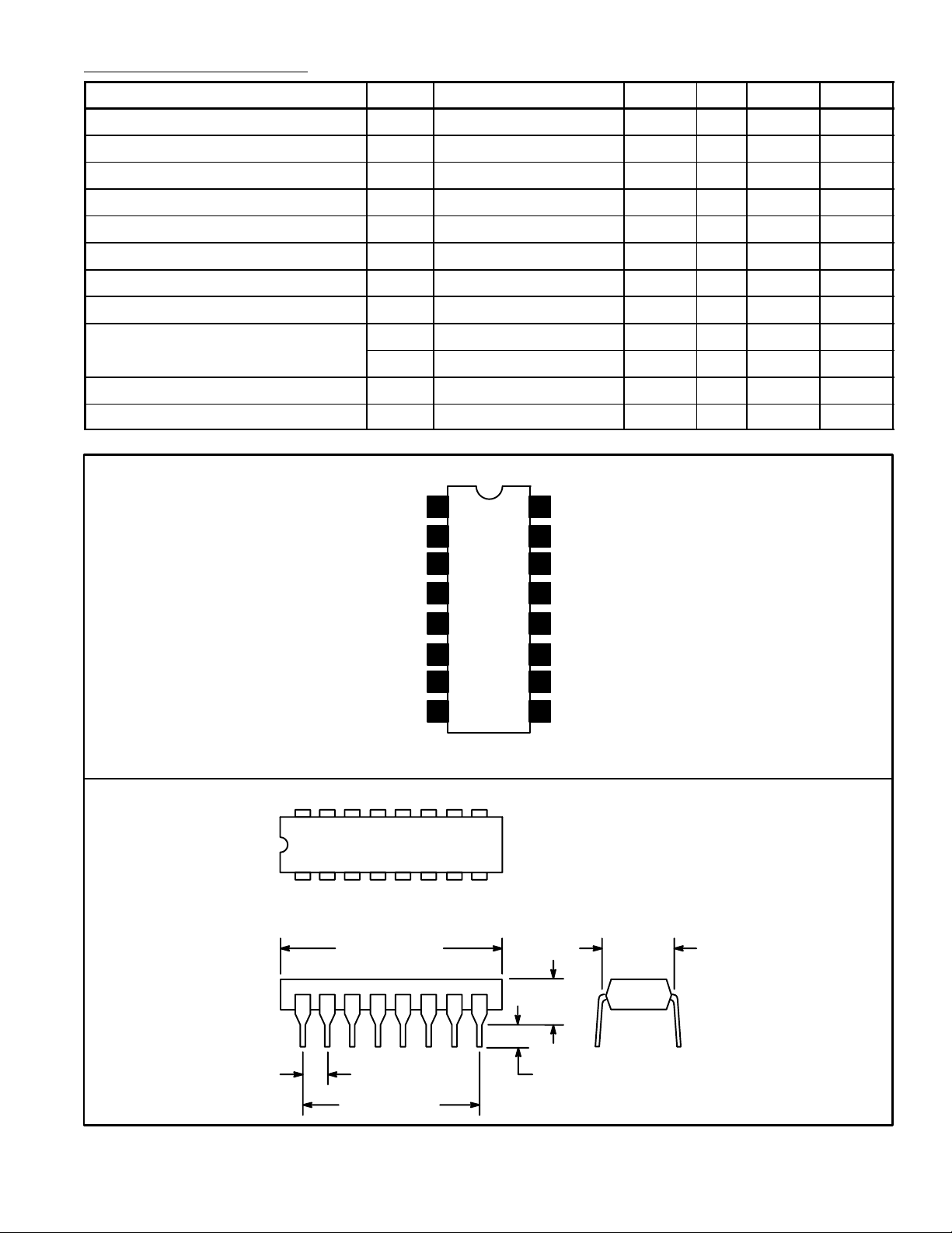
Pin Connection Diagram
O
1
I
1
= 50V, TA = +85°C – – 100 µA
OUT
= 4.5V, I
VR = 50V – – 50 µA
IF = 1.25A – 1.5 – V
= 5.5V, VIN = 0V – 8.5 12.5 mA/Gate
= 5.5V, VIN = V
VCC = 5V, RL = 43Ω – 0.2 – µs
V
= 50V, CL = 15pF – 5.0 – µs
OUT
1
2
3
4
OUT
16
15
14
13
VCC–1.6 – 25 V
0 – VCC–3.6 V
– – 10 µA
= 0.7A – 1.3 1.8 V
CC
– – 10 µA
Common1 *
O
4
I
4
GND/Heat SinkGND/Heat Sink
12
I
11
3
10
O
3
9
Common2 *
I
O
VCC 2
5
6
2
7
2
8
Note: These pins are internally connected.
16 9
18
.870 (22.0)
Max
.200 (5.08)
Max
.260 (6.6)
Max
.100 (2.54)
.700 (17.78)
.099 (2.5) Min
 Loading...