


NTE2032
Integrated Circuit
BCD–to–Seven–Segment Decoder Driver
Description:
The NTE2032 is a monolithic integrated circuit in a 16–Lead DIP type package that performs the
BCD–to–seven–segment decoding function and features constant–current segment drivers. When
used with the NTE2054 A/D converter , the NTE2032 provides a complete digital readout system with
a minimum number of external parts.
Features:
D TTL Compatible Input Logic Levels
D 25mA (Typ) Constant Current Segment Outputs
D Eliminates Need for Output Current Limiting Resistors
D Pin Compatible with Other Industry Standard Decoders
D Low Standby Power Dissipation: 18mW Typ
Absolute Maximum Ratings:
DC Supply Voltage (Between Pin1 and Pin10), V+ 7V. . . . . . . . . . . . . . . . . . . . . . . . . . . . . . . . . . . . . . .
Input Voltage (Pin1, Pin2, Pin6, and Pin7), V
Output Voltage, V
O
IN
Output “OFF” 7V. . . . . . . . . . . . . . . . . . . . . . . . . . . . . . . . . . . . . . . . . . . . . . . . . . . . . . . . . . . . . . . . .
Output “ON” (Note 1) 10V. . . . . . . . . . . . . . . . . . . . . . . . . . . . . . . . . . . . . . . . . . . . . . . . . . . . . . . . .
Device Dissipation (TA ≤ +55°C), P
D
Derate Above 55°C 10.5mW/°C. . . . . . . . . . . . . . . . . . . . . . . . . . . . . . . . . . . . . . . . . . . . . . . . . . . .
Operating Ambient Temperature Range, T
Storage Temperature Range, T
stg
opr
–65° to +150°C. . . . . . . . . . . . . . . . . . . . . . . . . . . . . . . . . . . . . . . . . .
Lead Temperature (During Soldering, 1.16” ±1/32” (1.59mm ±0.79mm), 10sec max), T
0° to +75°C. . . . . . . . . . . . . . . . . . . . . . . . . . . . . . . . . . . .
L
5.5V. . . . . . . . . . . . . . . . . . . . . . . . . . . . . . . . . . . . . . . .
1W. . . . . . . . . . . . . . . . . . . . . . . . . . . . . . . . . . . . . . . . . . . . . . . . . .
+265°C. .
Note 1. This is the maximum output voltage for any single output. The output voltage must be consis-
tent with the maximum dissipation and worst case conditions. Example: All segments “ON”,
100% duty cycle.
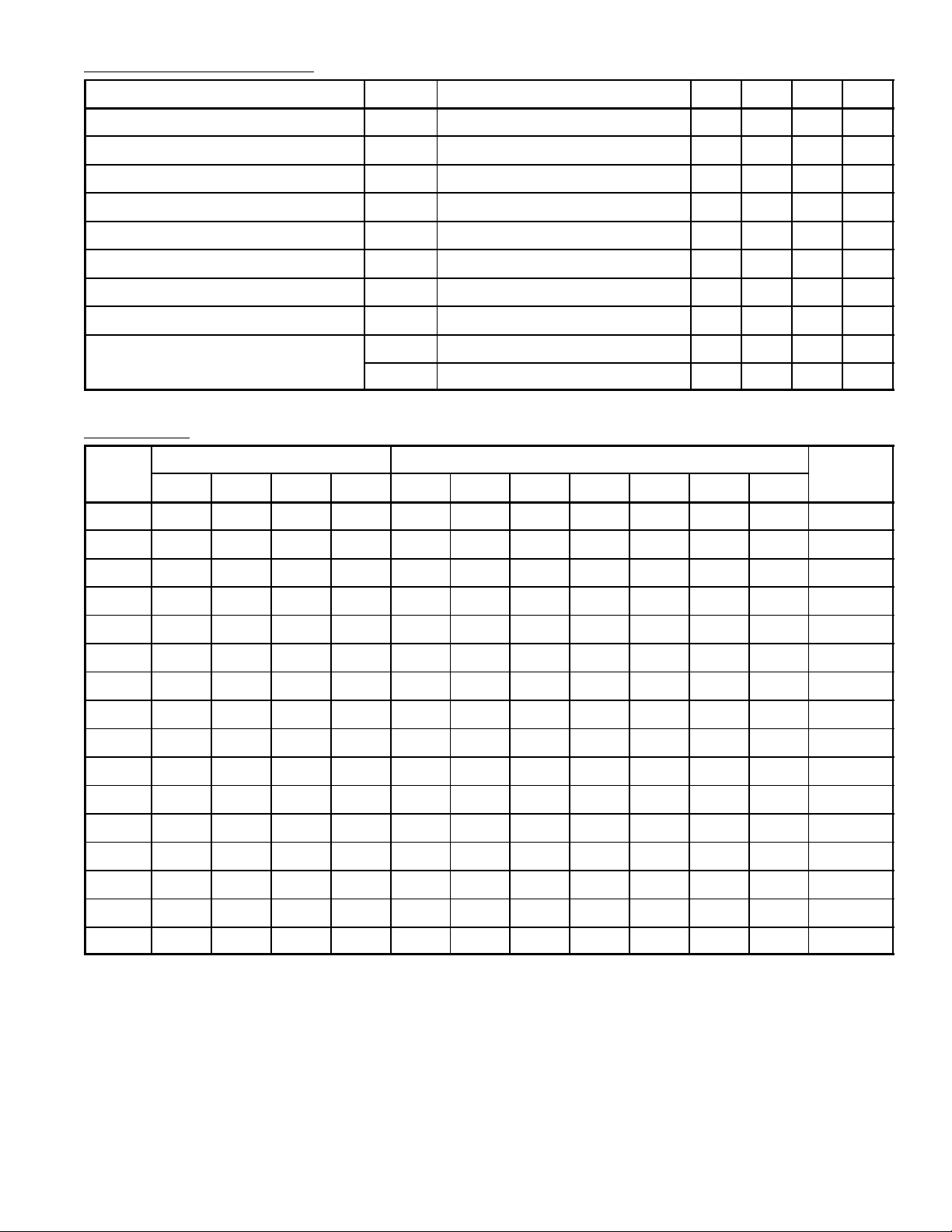
Electrical Characteristics: (TA = +25°C unless otherwise specified)
Parameter Symbol Test Conditions Min Typ Max Unit
Supply Voltage Operating Range V+ 4.5 5.0 5.5 V
Supply Current I+ All Inputs High – 3.5 8.0 mA
Output Current Low VO = 2V 18 25 32 mA
Output Current High VO = 5.5V – – 250 µA
Input Voltage High (Logic “1” Level) 2 – – V
Input Voltage Low (Logic “0” Level) – – 0.8 V
Input Current High (Logic “1”) 2V –30 – – µA
Input Current Low (Logic “0”) 0V –40 – – µA
Propagation Delay Time t
PHL
t
PLH
– 2.6 – µs
– 1.4 – µs
Truth Table:
Binary
Binary
State
3
2
0 L L L L L L L L L L H 0
1 L L L H H L L H H H H 1
2 L L H L L L H L L H L 2
3 L L H H H L L L H H L 3
4 L H L L L L L H H L L 4
5 L H L H H H L L H L L 5
6 L H H L L H L L L L L 6
7 L H H H H L L H H H H 7
8 H L L L L L L L L L L 8
9 H L L H H L L L H L L 9
10 H L H L L H H H H H L –
Inputs Outputs
2
2
1
2
0
2
a b c d e f g
Displays
11 H L H H H H H L L L L E
12 H H L L L L L H L L L H
13 H H L H H H H L L L H L
14 H H H L L L H H L L L P
15 H H H H H H H H H H H Blank
 Loading...