

NTE2030
Integrated Circuit
High Voltage Segment Driver for
Gas Discharge Tubes
Description:
The NTE2030 is capable of driving 8 segments of a high voltage display tube with a constant output
sink current, which can be adjusted by external program resistor, Rp. The program current is half that
of output “ON” current. In the “OFF” state the outputs can tolerate more than 80V. The ratio of “ON”
output currents is within ±10%. Inputs have negative clamp diodes. Active high input logic. The main
application of the device is to interface MOS circuits to high-voltage displays.
Features:
D Versatile Circuits for a Wide Range of Display Applications
D High Breakdown Voltages
D Low Power Dissipation
Absolute Maximum Ratings;
Input Voltage (Note 2) -20V. . . . . . . . . . . . . . . . . . . . . . . . . . . . . . . . . . . . . . . . . . . . . . . . . . . . . . . . . . . . .
Output Voltage 85V. . . . . . . . . . . . . . . . . . . . . . . . . . . . . . . . . . . . . . . . . . . . . . . . . . . . . . . . . . . . . . . . . . . . .
Operating Temperature Range 0° to +70°C. . . . . . . . . . . . . . . . . . . . . . . . . . . . . . . . . . . . . . . . . . . . . . . .
Storage Temperature Range -65° to +150°C. . . . . . . . . . . . . . . . . . . . . . . . . . . . . . . . . . . . . . . . . . . . . . .
Lead Temperature (During Soldering, 10sec) +300°C. . . . . . . . . . . . . . . . . . . . . . . . . . . . . . . . . . . . . . .
Note 1 “Absolute Maximum Ratings” are those values beyond which the safety of the device cannot
be guaranteed. Except “Operating Temperature Range” they are note meant to imply that
the devices should be operated at these limits. The table of “Electrical Characteristics” provides conditions for actual device operation.
Note 2 All voltage for NTE2030 with respect to VCC = 0V.
DC Electrical Characteristics: (Note 2 & Note 3)
Parameter Symbol Test Conditions Min Typ Max Unit
Input Current I
Logical “0” Input Current I
Logical “1” Input Current I
Input Clamp Voltage V
VIN = 6.0V 150 250 350 µA
I
I
IL
IH
I
= 5.0µA, V
OUT
I
= 1.4mA, IIP = 850µA, V
OUT
IIN = -1.0mA, TA = +25°C - -0.68 -0.85 V
= 75V - - 7.0 µA
OUT
= 50V 80 - - µA
OUT
Note 2 All voltage for NTE2030 with respect to VCC = 0V.
Note 3 Unless otherwise specified, Min/Max limits apply across the 0°C to +70°C. All typicals are
given for TA = +25°C.
DC Electrical Characteristics (Cont’d): (Note 2 & Note 3)
Parameter Symbol Test Conditions Min Typ Max Unit
Output Breakdown Voltage V
Output Leakage Current I
Prog Input Voltage I
Logical “0” Output Current I
Output Current Ratio ∆I
PROGIIP
CEX
OL
OH
O
I
= 100µA, IIN = 0µA 80 - - V
OUT
V
= -75V, -0.1mA ≤ IIN ≤ 7.0µA - 0.02 5.0 µA
OUT
= 150µA
V
= 50V,
OUT
80µA ≤ IIN ≤ I
I
b Ref = 1.7mA, V
OUT
IIP = 150µA 240 300 360 µA
IP
I
= 400µA 680 800 920 µA
IP
IIP = 850µA 1.53 1.7 1.87 mA
= 50V 0.9 1.0 1.1
OUT
1.8 2.3 -
- 4.0 4.5
V
Note 2 All voltage for NTE2030 with respect to VCC = 0V.
Note 3 Unless otherwise specified, Min/Max limits apply across the 0°C to +70°C. All typicals are
given for TA = +25°C.
Note 4 Supply currents specified for any one input = -1.0V. All other inputs = -5.5V and selected
output having 16mA load.
AC Electrical Characteristics: (TA = +25°C, unless otherwise indicated)
Parameter Symbol Test Conditions Min Typ Max Unit
Propagation Delay to a Logical
“0” from Input to Output
t
pd0
RP = 6k to 6V, R
= 1k to 6V - 37 100 ns
OUT
Propagation Delay to a Logical
“1” from Input to Output
t
pd1
Input Ramp Rate ≤ 15ns, Freq = 1MHz,
DC = 50%, Amplitude = 6.0V
- 92 200 ns
Note 2 All voltage for NTE2030 with respect to VCC = 0V.
Note 3 Unless otherwise specified, Min/Max limits apply across the 0°C to 70°C. All typicals are
given for TA = +25°C.
Note 4 Supply currents specified for any one input = -1.0V. All other inputs = -5.5V and selected
output having 16mA load.
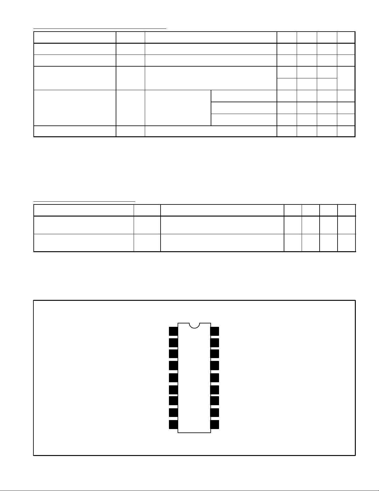
Pin Connection Diagram
Current
Input 1
Input 2
Input 3
1
2
3
4
5Input 4
6Input 5
7Input 6
8Input 7
18
V
DD
17
Output 2
16
Output 3
15
Output 4
14 Output 5
13 Output 6
Output 7
12
Output 8
11
Input 8
Substrate (GND)9 10
 Loading...