


NTE2027
Integrated Circuit
Hex LED Digit Driver
Description:
The NTE2027 is an interface circuit in a 14–Lead DIP typ package designed to be used in conjunction
with MOS integrated circuits and common cathode LED’s in serially addressed multi–digit displays.
The number of drivers required for this time–multiplexed system is minimized as a result of the segment–address–and–digit–scan method of LED drive.
Features:
D Sink Capability Per Driver: 350mA
D MOS Compatibility (Low Input Current)
D Low Standby Power
D High–Gain Darlington Circuits
Absolute Maximum Ratings: (Note 1)
Input Voltage Range (Note 2) –5V to V
Collector Output Voltage 10V. . . . . . . . . . . . . . . . . . . . . . . . . . . . . . . . . . . . . . . . . . . . . . . . . . . . . . . . . . . .
Collector Output to Input Voltage 10V. . . . . . . . . . . . . . . . . . . . . . . . . . . . . . . . . . . . . . . . . . . . . . . . . . . . .
Voltage at VSS Pin (with Respect to Any Other Device Pin) 10V. . . . . . . . . . . . . . . . . . . . . . . . . . . . . .
Collector Output Current
Each Collector Output 350mA. . . . . . . . . . . . . . . . . . . . . . . . . . . . . . . . . . . . . . . . . . . . . . . . . . . . .
All Collector Outputs 600mA. . . . . . . . . . . . . . . . . . . . . . . . . . . . . . . . . . . . . . . . . . . . . . . . . . . . . . .
Continuous Total Dissipation 800mW. . . . . . . . . . . . . . . . . . . . . . . . . . . . . . . . . . . . . . . . . . . . . . . . . . . . . .
Operating Temperature Range 0° to +70°C. . . . . . . . . . . . . . . . . . . . . . . . . . . . . . . . . . . . . . . . . . . . . . . .
Storage Temperature Range –65° to +150°C. . . . . . . . . . . . . . . . . . . . . . . . . . . . . . . . . . . . . . . . . . . . . . .
Lead Temperature (During Soldering, 10sec) +300°C. . . . . . . . . . . . . . . . . . . . . . . . . . . . . . . . . . . . . . .
. . . . . . . . . . . . . . . . . . . . . . . . . . . . . . . . . . . . . . . . . . . . . . . . . .
SS
Note 1. “Absolute Maximum Ratings” are those values beyond which the safety of the device cannot
be guaranteed. Except for “Operating Temperature Range” they are not meant to imply that
the device should be operated at these limits. The table of “Electrical Characteristics” provides conditions for actual device operation.
Note 2. The input is the only device pin which may be negative with respect to GND.
DC Electrical Characteristics: (VSS = 10V, TA = 0° to +70°C, Note 3, Note 4 unless otherwise
specified)
Parameter Symbol Test Conditions Min Typ Max Unit
Low Level Output Voltage V
High Level Output Current I
OH
Input = 6.5V through 1kΩ,
OL
I
= 350mA, TA = +25°C
OUT
Input = 6.5V through 1kΩ,
I
= 350mA
OUT
– 1.2 1.4 V
– – 1.6 V
VOH = 10V, IIN = 40µA – – 200 µA
VOH = 10V, VIN = 0.5V – – 200 µA
Input Current at Max Input Voltage I
Current into VSS Pin I
SS
VIN = 10V, IOL = 20mA – 2.2 3.3 mA
I
– – 1.0 mA
Note 3. Unless otherwise specified, Min/Max limits apply across the 0° to +70°C temperature range.
Note 4. All currents into device pins shown as positive, out of device as negative, all voltages refer-
enced to GND unless otherwise specified. All values shown as mmax or Min on absolute
value basis.
AC Switching Characteristics (VSS = 7.5V, TA = +25°C unless otherwise specified)
Parameter Symbol Test Conditions Min Typ Max Unit
Propagation Delay Time
Low–to–High Level Output t
High–to–Low Level Output t
PLH
PHL
VIH = 7.5V, RL = 39Ω, CL = 15pF
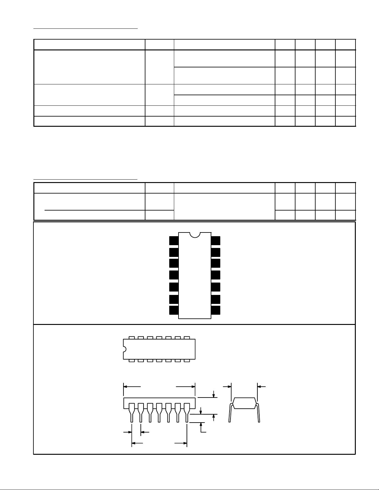
Pin Connection Diagram
– 300 – ns
– 30 – ns
1Y
1
2
2Y
3
2A
GND
3A
4
5
63Y
74Y
14 8
17
.785 (19.95)
Max
.200 (5.08)
14
13
12
11
10
9
8 4A
Max
1A
6Y
6A
V
5A
5Y
SS
.300
(7.62)
.100 (2.45) .099 (2.5) Min
.600 (15.24)
 Loading...