


NTE2024
Integrated Circuit
2–Digit BCD–to–7–Segment Decoder/Driver
Features:
D Separate BCD inputs and segment outputs for each digit
D Input loading less than 15µA
D I2L logic with buffered inputs and outputs
D Internal input overrange protection circuit
D 5V supply operation
D Internal biasing circuits
D Output drive capability of 25mA per segment
D Open collector outputs drive indicators directly
Description:
The NTE2024 is a monolithic integrated circuit intended for 2–digit display such as “numbers” for tV
and “CB” channel selection, and other 0–99 numerical or counting for consumer or industrial indicator
applications. It consists of two independent BCD–to–7 segment decoder/drivers. Two sets of BCD
inputs are buffered with p–n–p differential amplifier stages internally referenced to 1.7V. Each of the
eight input terminals draws less than 15µA and is provided with an internal protection circuit.
Decoding is accomplished with I2L ROM’s. The fourteen output terminals are buffered with Darlington
pairs driving common–emitter output transistors. Each output is capable of sinking 25mA for an LED
common–anode display device. The supply–voltage range (VCC) is intended to be 4.5V to 6V. The
output voltage (VO) must not exceed 12V, which provides for a wide range of common–anode voltage
sources.
Absolute Maximum Ratings:
Supply Voltage, VCC 6V. . . . . . . . . . . . . . . . . . . . . . . . . . . . . . . . . . . . . . . . . . . . . . . . . . . . . . . . . . . . . . . .
Input–Voltage (Min/Max) –0.3VCC V. . . . . . . . . . . . . . . . . . . . . . . . . . . . . . . . . . . . . . . . . . . . . . . . . . . . . .
Input Current (Protection Circuit) ±10mA. . . . . . . . . . . . . . . . . . . . . . . . . . . . . . . . . . . . . . . . . . . . . . . . . .
Output Voltage, VO 12V. . . . . . . . . . . . . . . . . . . . . . . . . . . . . . . . . . . . . . . . . . . . . . . . . . . . . . . . . . . . . . . .
Output Segment Current, I
Display
Power Dissipation (TA ≤ +70°C), P
25mA. . . . . . . . . . . . . . . . . . . . . . . . . . . . . . . . . . . . . . . . . . . . . . . . . . .
D
400mW. . . . . . . . . . . . . . . . . . . . . . . . . . . . . . . . . . . . . . . . . . . . . . .
Derate Linearly Above +70°C 8.7mW/°C. . . . . . . . . . . . . . . . . . . . . . . . . . . . . . . . . . . . . . . . . . .
Operating Ambient temperature Range, T
StorageTemperature range, T
stg
Lead Temperature (During Soldering, 1/16” ± 1/32” from case, 10sec max), T
0° to 70°C. . . . . . . . . . . . . . . . . . . . . . . . . . . . . . . . . . . .
opr
L
–55° to +150°C. . . . . . . . . . . . . . . . . . . . . . . . . . . . . . . . . . . . . . . . . . . .
+265°C. . . . . . . . . .
Electrical Characterisitic: (VCC = 5V, V1 = GND, V
specified)
Parameter Symbol Test Conditions Min Typ Max Unit
= 12V, and TA = +25°C unless otherwise
DISP
Input Voltage, High V
Input Voltage, Low V
Input Current, High I
Input Current, Low I
On–State Output Voltage V
Off–State Output Current I
Power Supply Drain Current I
Input Capacitance C
MSD BCD
Inputs
MSD Segment
Outputs
IH
IL
IH
OL
OL
CC
All BCD Inputs = 5V – – 15 µA
All BCD Inputs = 0V –10 – – µA
IL
I
= 25mA – – 1 V
O(Sink)
VCC = 6V – 17 25 mA
I
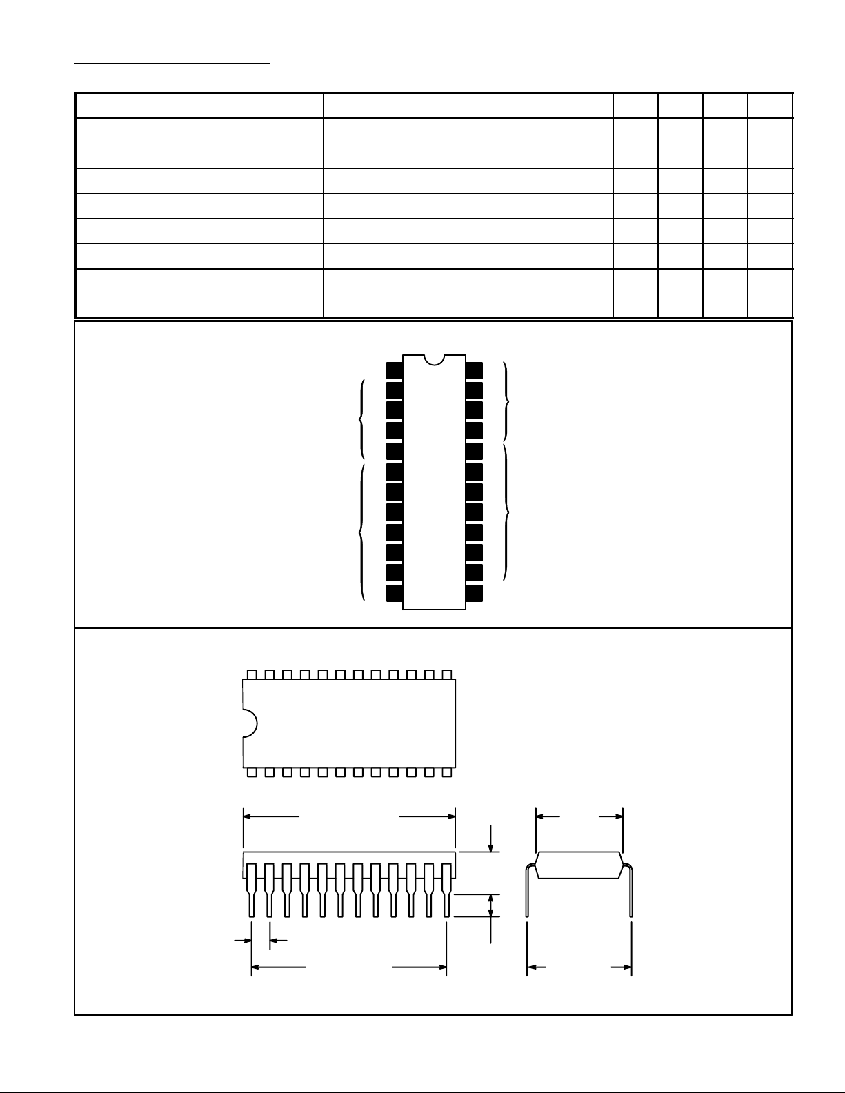
Pin Connection Diagram
GND
1
2
A
3
B
4
C
5D
6a
7
b
8c
9
d
10
e
11
f
12 13
g
24
23
22
21CD
20
19 b
18
17
16
15
14
V
A
B
a
c
d
e
f
g
LSD BCD
Inputs
LSD Segment
Outputs
CC
2.4 5.0 V
CC
0 – 0.6 V
– 5 50 µA
– 5 – [pF
V
24 13
112
1.300 (33.02)
Max
.100 (2.54)
1.100 (27.94)
.225
(5.73)
Max
.126
(3.22)
Min
.520
(13.2)
.600
(15.24)
 Loading...