

NTE2023
Integrated Circuit
General Purpose, High Current
7–Segment Display Driver
Description:
The NTE2023 is a general purpose high current transistor array in a 16–Lead DIP type package comprised of seven high current silicon NPN transistor on a common monolithic substrate. It is connected
in a common–collector configuration.
Absolute Maximum Ratings:
Power Dissipation (Any One Transistor), P
Operating Ambient Temperature Range, T
D
opr
–40° to +85°C. . . . . . . . . . . . . . . . . . . . . . . . . . . . . . . . . .
Individual Transistor Ratings:
Collector–Emitter Voltage, V
Collector–Base Voltage, V
Collector–Substrate Voltage, V
Emitter–Base Voltage, V
Collector Current, I
Base Current, I
C
B
CEO
CBO
CIO
EBO
Note 1. The collector of each transistor in the NTE2023 is isolated from the substrate by an integral
diode. The substrate must be connected to a voltage which is more negative than any collector voltage so as to maintain isolation between transistors, and to provide normal transistor
action. Undesired coupling between transistors is avoided by maintaining the substrate (5)
at either DC or signal (AC) ground. An appropriate bypass capacitor can be used to establish
a signal ground.
500mW. . . . . . . . . . . . . . . . . . . . . . . . . . . . . . . . . . . . . . . .
16V. . . . . . . . . . . . . . . . . . . . . . . . . . . . . . . . . . . . . . . . . . . . . . . . . . . . . .
20V. . . . . . . . . . . . . . . . . . . . . . . . . . . . . . . . . . . . . . . . . . . . . . . . . . . . . . .
20V. . . . . . . . . . . . . . . . . . . . . . . . . . . . . . . . . . . . . . . . . . . . . . . . . . . .
5V. . . . . . . . . . . . . . . . . . . . . . . . . . . . . . . . . . . . . . . . . . . . . . . . . . . . . . . . . .
200mA. . . . . . . . . . . . . . . . . . . . . . . . . . . . . . . . . . . . . . . . . . . . . . . . . . . . . . . . . . . . .
20mA. . . . . . . . . . . . . . . . . . . . . . . . . . . . . . . . . . . . . . . . . . . . . . . . . . . . . . . . . . . . . . . . .
Electrical Characteristics: (TA = +25°C unless otherwise specified)
Parameter Symbol Test Conditions Min Typ Max Unit
Collector–Emitter Breakdown Voltage V
Collector–Substrate Breakdown Voltage V
Collector–Emitter Breakdown Voltage V
Emitter–Base Breakdown Voltage V
Forward Current Transfer Ratio h
(BR)CESIC
(BR)CIEICI
(BR)CEOIC
(BR)EBOIC
FE
= 500µA 20 80 – V
= 500µA 20 80 – V
= 1mA 16 40 – V
= 500µA 5 7 – V
VCE = 0.5V, IC = 30mA 30 80 –
VCE = 0.8V, IC = 50mA 40 85 –
Electrical Characteristics (Cont’d): (TA = +25°C unless otherwise specified)
Parameter Symbol Test Conditions Min Typ Max Unit
Base–Emitter Saturation Voltage V
Collector–Emitter Saturation Voltage V
Collector Cutoff Current
Q1 Emitter
Q2 Emitter
Q2 Base
Q5 Emitter
Substrate
Q6 Emitter
Q6 Base
BE(sat)IC
CE(sat)
= 30mA – 0.75 1 V
IC = 30mA – 0.13 0.5 V
IC = 50mA – 0.2 0.7 V
I
CEO
I
CBO
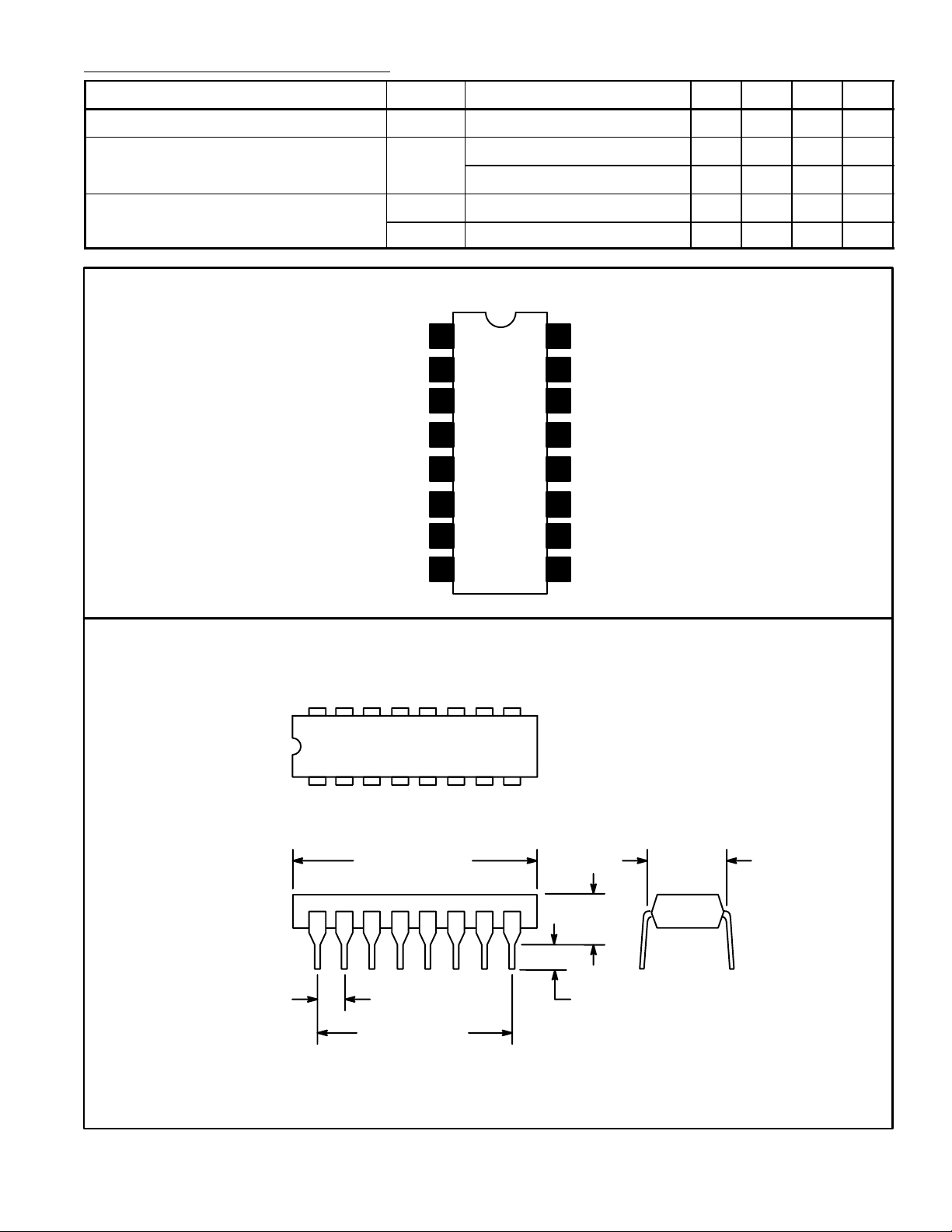
Pin Connection Diagram
VCE = 10V – – 10 µA
VCB = 10V – – 1 µA
1
2
3
4
5
6Q5 Base
7
8
16
15
14
13
12
11
10
9
V
DD
Common Cathode
Q3 Emitter
Q3 Base
Q4 Emitter
Q4 Base
Q7 Base
Q7 Emitter
16 9
18
.870 (22.0)
Max
.100 (2.54)
.700 (17.78)
.200 (5.08)
Max
.099 (2.5) Min
.260
(6.6)
Max
 Loading...