

NTE NTE2021, NTE2022 Datasheet
NTE2021 & NTE2022
Integrated Circuit
8–Digit/Segment Fluorescent Display Driver
Description:
The NTE2021 and NTE2022 consist of eight NPN Darlington output stages and the associated common–emitter input stages in an 18–Lead DIP type package. These devices are designed to interface
between low–level digital logic and vacuum fluorescent displays. They are capable of driving the digits and/or segments of these displays and are designed to permit all outputs to be activated simultaneously. Pulldown resistors are incorporated into each output and no external components are required for most fluorescent displays.
The NTE2020 is compatible with TTL, Schottky TTL, DTL and 5V CMOS. The NTE2021 device is
intended for use with MOS (PMOS & CMOS) logic operating from supply voltages of 6V to 15V.
Features:
D Digit or Segment Drivers
D Low Input Current
D Integral Output Pull–Down Resistors
D Low Power
D Reliable Monolithic Construction
D High Output Breakdown Voltage
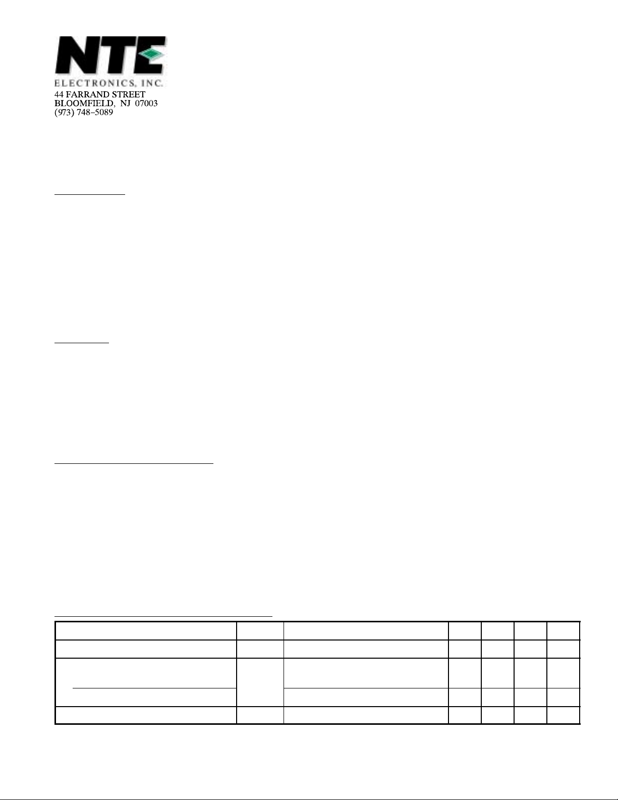
Absolute Maximum Ratings: (TA = +25°C, Note 1)
Supply Voltage, V
Input Voltage, V
Output Current, I
BB
IN
OUT
Allowable Power Dissipation, P
D
85V. . . . . . . . . . . . . . . . . . . . . . . . . . . . . . . . . . . . . . . . . . . . . . . . . . . . . . . . . . . . . . . .
20V. . . . . . . . . . . . . . . . . . . . . . . . . . . . . . . . . . . . . . . . . . . . . . . . . . . . . . . . . . . . . . . . . .
–40mA. . . . . . . . . . . . . . . . . . . . . . . . . . . . . . . . . . . . . . . . . . . . . . . . . . . . . . . . . . . . .
1W. . . . . . . . . . . . . . . . . . . . . . . . . . . . . . . . . . . . . . . . . . . . . . . . . . . . .
Derate Above 25°C 8.0mW/°C. . . . . . . . . . . . . . . . . . . . . . . . . . . . . . . . . . . . . . . . . . . . . . . . . . . . .
Operating Temperature Range, T
Storage Temperature Range, T
stg
A
–20° to +85°C. . . . . . . . . . . . . . . . . . . . . . . . . . . . . . . . . . . . . . . . . . .
–55° to +150°C. . . . . . . . . . . . . . . . . . . . . . . . . . . . . . . . . . . . . . . . . .
Note 1. Voltages are with reference to GND unless otherwise specified
Recommended Operating Conditions:
Parameter Symbol Test Conditions Min Typ Max Unit
Supply Voltage V
Input ON Voltage
NTE2021
NTE2022 4.0 – 15 V
Output ON Current I
BB
V
IN
OUT
5 – 70 V
2.4 – 15 V
– – –25 mA
Note 2. Positive (negative) current is defined as going into (coming out of) the specified device pin.
Electrical Characteristics: (TA = –20° to +85°C, VBB = 80V unless otherwise specified)
Parameter Symbol Test Conditions Min Typ Max Unit
Output Leakage Current I
OUT
Output OFF Voltage V
Output Pull–Down Current I
Output ON Voltage
OUT
V
NTE2021
NTE2022 V
Input ON Current
NTE2021
OUT
OUT
I
VIN = 400mV – – 15 µA
VIN = 400mV – – 1.0 V
V
= VBB, Input Open 450 650 1100 µA
OUT
V
IN
= 2.4V, I
IN
= 4.0V, I
IN
= –25mA 77 78 – V
OUT
= –25mA 77 78 – V
OUT
VIN = 2.4V – 120 225 µA
VIN = 5.0V – 375 650 µA
NTE2022 VIN = 4.0V – 130 250 µA
VIN = 15.0V – 675 1150 µA
Supply Current
NTE2021 & NTE2022
I
BB
All Inputs Open – 10 100 µA
NTE2021 All Inputs = 2.4V – 6.0 9.0 mA
NTE2022 All Inputs = 4.0V – 6.0 9.0 mA
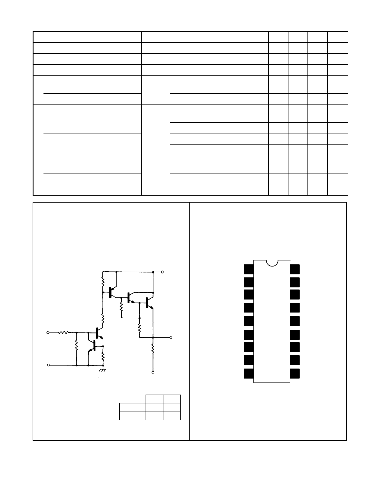
Partial Schematic
(One Driver)
Pin Connection Diagram
Input
GND
V
BB
30k
Input 1
Input 2
Input 3
27k
R
IN
R
B
15k
Output
125k
Input 4
1
2
3
4
5Input 5
6Input 6
7Input 7
8Input 8
V
EE
R
NTE2021 10kΩ 30kΩ
NTE2022 20kΩ 20kΩ
R
IN
B
GND
9 10
Output 1
18
17
Output 2
16
Output 3
15
Output 4
14 Output 5
13 Output 6
Output 7
12
Output 8
11
V
BB
 Loading...