

NTE NTE2020, NTE2018, NTE2019, NTE2016 Datasheet

NTE2016/NTE2017/NTE2018/NTE2019/NTE2020
Integrated Circuit
8–Channel Darlington Array/Driver
Description:
Ideally suited for interfacing between low–level digital logic circuitry and high–power peripheral loads,
the NTE2011 through NTE2015 are high–voltage, high–current Darlington arrays in an 18–Lead DIP
type package and feature peak load current ratings to 600mA (NTE2016, NTE2019) or 750mA
(NTE2017, NTE2018, NTE2020) for each of the eight drivers in each device. Under the proper conditions, high–power loads up to 4A at 50V (200W at 23% duty cycle) or 3.2A at 95V (304W at 33% duty
cycle) can be controlled. Typical loads include relays, solenoids, stepping motors, multiplexed LED
and incadescent displays, and heaters. All devices feature open collector outputs and integral diodes
for inductive load transient suppression.
The NTE2016 is a general purpose array that may be used with standard bi–polar digital logic using
external current limiting, or with most PMOS or CMOS directly. This device is pinned with outputs
opposite inputs to facilitate printed wiring board layouts.
The NTE2017 is designed for use with 14V to 25V PMOS devices. Each input has a Zener diode and
resistor in series to limit the input current to a safe value in that application. The Zener diode also gives
this deVicee excellent noise immunity.
The NTE2018 has a 2.7kΩ series base resistor for each Darlington pair, allowing operation directly
with TTL or CMOS operating at a supply voltage of 5V. This device will handle numerous interface
needs – particularly those beyond the capabilities of standard logic buffers.
The NTE2019 has a 10.5kΩ series input resistor that permits operation directly from CMOS or PMOS
outputs utilizing supply voltages of 6V to 15V. The required input current is below that of the NTE2018,
while the required input voltage is less than that required by the NTE2017.
The NTE2020 is designed for use with standard TTL and Schottky TTL, with which higher output currents are required and loading of the logic output is not a concern. This device will sink a minimum
of 350mA when driven from a “totem pole” logic output.
Absolute Maximum Ratings: (TA = +25°C for any one Darlington pair unless otherwise specified)
Output Voltage, V
Input Voltage, V
IN
CE
50V. . . . . . . . . . . . . . . . . . . . . . . . . . . . . . . . . . . . . . . . . . . . . . . . . . . . . . . . . . . . . . . .
NTE2017, NTE2018, NTE2019 30V. . . . . . . . . . . . . . . . . . . . . . . . . . . . . . . . . . . . . . . . . . . . . . . .
NTE2020 15V. . . . . . . . . . . . . . . . . . . . . . . . . . . . . . . . . . . . . . . . . . . . . . . . . . . . . . . . . . . . . . . . . . . .
Continuous Collector Current. I
C
NTE2016, NTE2019 500mA. . . . . . . . . . . . . . . . . . . . . . . . . . . . . . . . . . . . . . . . . . . . . . . . . . . . . . .
NTE2017, NTE2018, NTE2020 600mA. . . . . . . . . . . . . . . . . . . . . . . . . . . . . . . . . . . . . . . . . . . . .
Continuous Base Current, I
Power Dissipation, P
D
B
25mA. . . . . . . . . . . . . . . . . . . . . . . . . . . . . . . . . . . . . . . . . . . . . . . . . . . . . . .
One Darlington Pair 1W. . . . . . . . . . . . . . . . . . . . . . . . . . . . . . . . . . . . . . . . . . . . . . . . . . . . . . . . . .
Total Device (Note 1) 2.25W. . . . . . . . . . . . . . . . . . . . . . . . . . . . . . . . . . . . . . . . . . . . . . . . . . . . . . .
Operating Ambient Temperature Range, T
Storage Temperature Range, T
stg
A
–20° to +85°C. . . . . . . . . . . . . . . . . . . . . . . . . . . . . . . . . . .
–55° to +150°C. . . . . . . . . . . . . . . . . . . . . . . . . . . . . . . . . . . . . . . . . .
Note 1. Derate at the rate of 18.18mW/°C above +25°C.
Note 2. Under normal operating conditions, these devices will sustain 350mA per output with
V
CE(sat)
= 1.6V at +50°C with a pulse width of 20ms and a duty cycle of 40%.
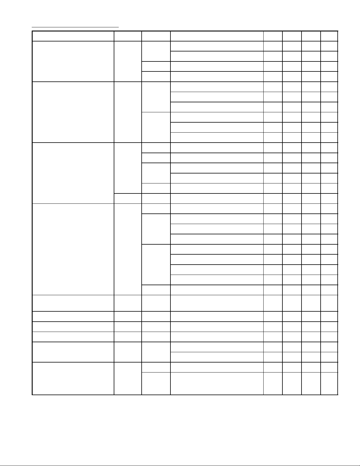
Electrical Characteristics: (TA = +25° unless otherwise specified)
Parameter Symbol Device Test Conditions Min Typ Max Unit
Output Leakage Current I
Collector–Emitter V
CEX
CE(sat)
Saturation Voltage NTE2019
Input Current I
Input Voltage V
IN(ON)
I
IN(OFF)
IN(ON)
All VCE = 50V, TA = +25°C – – 50 µA
VCE = 50V, TA = +70°C – – 100 µA
NTE2017 VCE = 50V, TA = +70°C, VIN = 6V – – 500 µA
NTE2019 VCE = 50V, TA = +70°C, VIN = 1V – – 500 µA
NTE2016
IC = 100mA, IB = 250µA – 0.9 1.1 V
IC = 200mA, IB = 350µA – 1.1 1.3 V
IC = 350mA, IB = 500µA – 1.3 1.6 V
NTE2017
NTE2018
NTE2020
NTE2020
IC = 200mA, IB = 350µA – 1.1 1.3 V
IC = 350mA, IB = 500µA – 1.3 1.6 V
IC = 500mA, IB = 600µA – 1.7 1.9 V
NTE2017 VIN = 17V – 0.82 1.25 mA
NTE2018 VIN = 3.85V – 0.93 1.35 mA
NTE2019 VIN = 5V – 0.35 0.50 mA
VIN = 12V – 1.0 1.45 mA
NTE2020 VIN = 3V – 1.5 2.4 mA
All IC = 500µA, TA = +70°C 50 60 – µA
NTE2017 VCE = 2V, IC = 500mA – – 17 V
NTE2018 VCE = 2V, IC = 250mA – – 2.7 V
DC Forward Current
h
Transfer Ratio
Input Capacitance C
Turn–On Delay t
Turn–Off Delay t
Clamp Diode Leakage I
Current
Clamp Diode Forward Voltage V
FE
IN
PLH
PHL
R
VCE = 2V, IC = 300mA – – 3.0 V
VCE = 2V, IC = 500mA – – 3.5 V
NTE2019 VCE = 2V, IC = 125mA – – 5.0 V
VCE = 2V, IC = 200mA – – 6.0 V
VCE = 2V, IC = 275mA – – 7.0 V
VCE = 2V, IC = 350mA – – 8.0 V
NTE2020 VCE = 2V, IC = 350mA – – 2.6 V
NTE201 1 VCE = 2V, IC = 350mA 1000 – –
All – 15 25 pF
All 0.5 Ein to 0.5 E
All 0.5 Ein to 0.5 E
All
VR = 50V, TA = +25°C – – 50 µA
out
out
– 0.25 1.0 µs
– 0.25 1.0 µs
VR = 50V, TA = +70°C – – 100 µA
F
All IF = 350mA – 1.7 2.0 V
NTE2017
IF = 500mA – 2.1 2.5 V
NTE2018
NTE2020
 Loading...