

NTE2003
Integrated Circuit
Dolby B–Type Noise Reduction Processor
Description:
The NTE2003 is a monolithic integrated circuit in a 16–Lead DIP type package specifically designed
to realized the Dolby B–type noise reduction system.
Features:
D Reduced distortion at high frequencies and high signal levels
D Improved transient stability
D Wide Operating Voltage Range
D Low Supply Current
Absolute Maximum Ratings:
Supply Voltage, V
Operating Temperature Range, T
Storage Temperature Range, T
CC
opr
stg
Lead Temperature (During Soldering, 10sec Max), T
0° to +70°C. . . . . . . . . . . . . . . . . . . . . . . . . . . . . . . . . . . . . . . . . . .
–65° to +150°C. . . . . . . . . . . . . . . . . . . . . . . . . . . . . . . . . . . . . . . . . .
L
24V. . . . . . . . . . . . . . . . . . . . . . . . . . . . . . . . . . . . . . . . . . . . . . . . . . . . . . . . . . . . . . . .
+300°C. . . . . . . . . . . . . . . . . . . . . . . . . . . . . . . .
Electrical Characteristics
: (VCC = 12V, TA = +25°C, NB 0dB refers to 580mV
Dolby level at
rms
Pin3 unless otherwise specified)
Parameter Test Conditions Min Typ Max Unit
Supply Voltage Range 9 – – V
Supply Current 12 17 22 mA
Voltage Gain
(Pin5–Pin3)
(Pin3–Pin7) 1kHz (Noise Reduction Out) –1 0 1 dB
Distortion 1kHz, 0dB; 10kHz, 10dB – 0.05 0.1 %
Signal Handling 1kHz 0.3% Distortion 10 14 – dB
Signal–to–Noise Ratio
Encode (CCIR Weighted)
Decode +75 80 – dB
1kHz Pin6 & Pin2 Connected 24 26 28 dB
Pin6 & Pin2 Connected, RS = 10kΩ
65 70 – dB
Electrical Characteristics (Cont’d): (VCC = 12V, TA = +25°C, NB 0dB refers to 580mV
rms
Dolby
level at Pin3 unless otherwise specified)
Parameter Test Conditions Min Typ Max Unit
Encode Characteristics (Input to Pin5) 1.3kHz, –20dB –17.2 –15.7 .14.2 dB
2.5kHz, –20dB –17.4 –15.9 –14.4 dB
3.0kHz, –30dB –22.7 –21.2 –19.7 dB
5.0kHz, –30dB –23.3 –21.8 –20.3 dB
10kHz, 0dB –1.0 0.5 2.0 dB
10kHz, –40dB –31.1 –29.6 –28.1 dB
14kHz, –30dB –25.4 –23.9 –22.4 dB
Back–to–Back Frequency Response With Standard Dolby B–Type Processor –1.5 0 1.5 dB
Input Resistance Pin5 45 65 85 kΩ
Pin2 4.3 5.6 6.9 kΩ
Output Resistance Pin6 1.8 2.4 3.0 kΩ
Pin3 – 80 120 kΩ
Pin7 – 80 120 kΩ
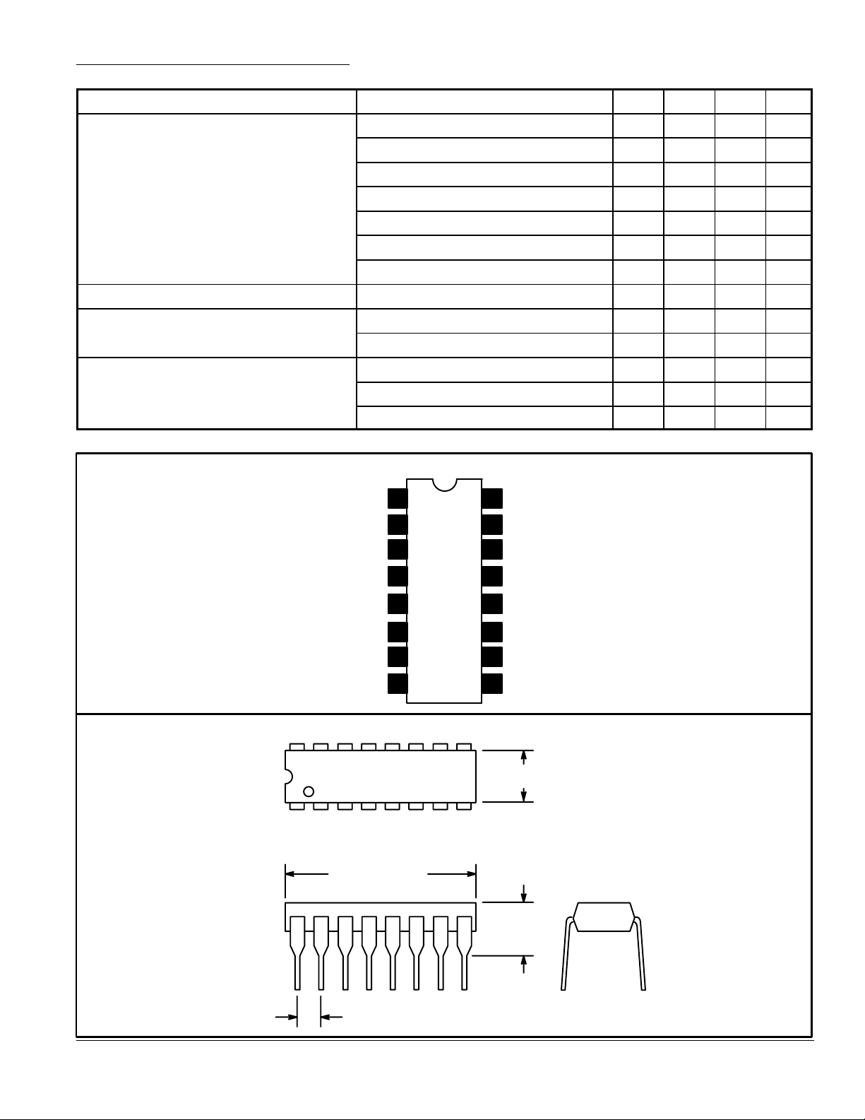
Pin Connection Diagram
Variable Impedance Input
Amp B Input
Amp B Output
Bias
Amp S Output
16 9
18
.850 (21.6
1
2
3
4
5Amp A Input
6Amp A Output
7
8Decoupling
16
V
CC
15
Variable Impedance Control
Rectifier Output
14
13
Rectifier Bias
12 Rectifier Input
11 Amp D Output
10
Amp D Feedback Decoupling
GND
9
.260 (6.6) Max
.100 (2.54)
.180
(4.0)
 Loading...