

NTE NTE199 Datasheet
NTE199
Silicon NPN Transistor
Low Noise, High Gain Amplifier
Description:
The NTE199 is a silicon NPN transistor in a TO92 type package designed especially for low noise
preamplifier and small signal industrial amplifier applications. This device features low collector saturation voltage, tight beta control, and excellent low noise characteristics.
Absolute Maximum Ratings: (TA = +25°C unless otherwise specified)
Collector–Emitter Voltage, V
Collector–Base Voltage, V
Emitter–Base Voltage, V
Steady State Collector Current (Note 1), I
Total Power Dissipation (T
CEO
CBO
EBO
= +25°C), P
A
C
T
Derate Above +25°C 3.3mW/°C. . . . . . . . . . . . . . . . . . . . . . . . . . . . . . . . . . . . . . . . . . . . . . . . . . . .
Total Power Dissipation (T
= +55°C), P
A
T
Derate Above +25°C 3.3mW/°C. . . . . . . . . . . . . . . . . . . . . . . . . . . . . . . . . . . . . . . . . . . . . . . . . . . .
Operating Junction Temperature Range, T
Storage Temperature Range, T
stg
J
Lead Temperature (During Soldering, 1/16” from case, 10sec max), T
–55° to +125°C. . . . . . . . . . . . . . . . . . . . . . . . . . . . . . . . . .
–55° to +150°C. . . . . . . . . . . . . . . . . . . . . . . . . . . . . . . . . . . . . . . . . .
L
50V. . . . . . . . . . . . . . . . . . . . . . . . . . . . . . . . . . . . . . . . . . . . . . . . . . . . . .
70V. . . . . . . . . . . . . . . . . . . . . . . . . . . . . . . . . . . . . . . . . . . . . . . . . . . . . . .
5V. . . . . . . . . . . . . . . . . . . . . . . . . . . . . . . . . . . . . . . . . . . . . . . . . . . . . . . . . .
100mA. . . . . . . . . . . . . . . . . . . . . . . . . . . . . . . . . . . . . . . . .
360mW. . . . . . . . . . . . . . . . . . . . . . . . . . . . . . . . . . . . . . . . . .
260mW. . . . . . . . . . . . . . . . . . . . . . . . . . . . . . . . . . . . . . . . . .
+260°C. . . . . . . . . . . . . . . . .
Note 1. Determined from power limitations due to saturation voltages at this current
Electrical Characteristics:
Parameter Symbol Test Conditions Min Typ Max Unit
Static Characteristics
Collector Cutoff Current I
Collector Cutoff Current I
Emitter Cutoff Current I
(TA = +25°C unless otherwise specified)
CBO
CES
EBO
VCB = 50V – – 30 nA
VCB = 50V, TA = +100°C – – 10 µA
VCB = 50V – – 30 nA
VEB = 5V – – 50 nA
Electrical Characteristics (Cont’d): (TA = +25°C unless otherwise specified)
Parameter Symbol Test Conditions Min Typ Max Unit
Static Characteristics (Cont’d)
Forward Current Transfer Ratio h
FE
VCE = 5V, IC = 2mA 400 – 800
VCE = 5V, IC = 100µA, Note 2 – 300 –
Breakdown Voltage
V
(BR)CEOIC
= 10mA, Note 3 50 – – V
Collector–to–Emitter
Breakdown Voltage
V
(BR)CBOIC
= 10µA 70 – – V
Collector–to–Base
Breakdown Voltage
V
(BR)EBOIE
= 10µA 5 – – V
Emitter–to–Base
Collector Saturation Voltage V
Base Saturation Voltage V
Base Emitter ON Voltage V
CE(sat)IC
BE(sat)IC
BE(on)
= 10mA, IB = 1mA, Note 3 – – 0.125 V
= 10mA, IB = 1mA, Note 3 – – 0.78 V
VCE = 10V, IC = 2mA 0.5 – 0.9 V
Dynamic Characteristics
Forward Current Transfer Ratio h
Output Capacitance,
fe
C
cb
VCE = 5V, IC = 2mA, f = 1kHz 400 – 1200
VCB = 10V, IE = 0, f = 1kHz – – 4 pF
Common Base
Noise Figure NF IC = 100µA, VCE = 5V,
= 5kΩ, f = 1kHz
R
g
– – 3 dB
Note 2. Typically, a minimum of 95% of the distribution is above this value.
Note 3. Pulse Test: Pulse Width ≤ 300µs, Duty Cycle ≤ 2%
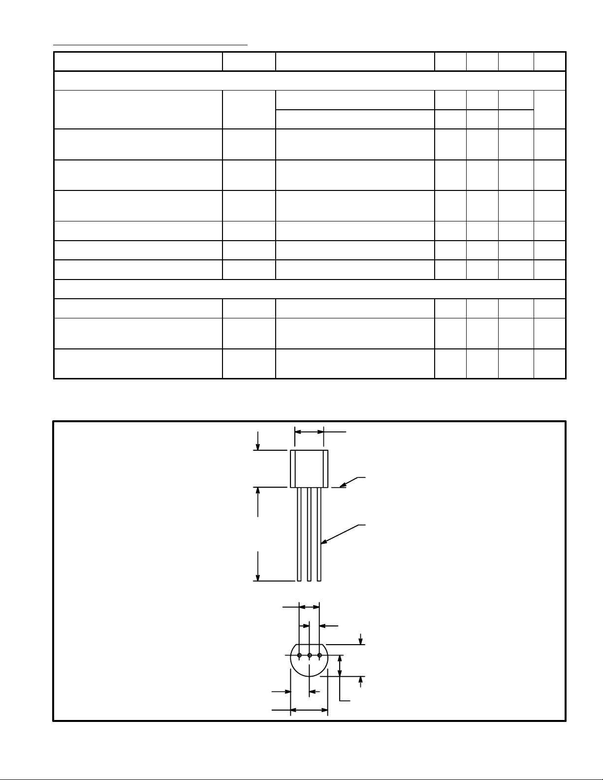
.135 (3.45) Min
.210
(5.33)
Max
.500
(12.7)
Min
E C B
.100 (2.54)
.050 (1.27)
Seating Plane
.021 (.445) Dia Max
.165
(4.2)
Max
.105 (2.67) Max
.205 (5.2) Max
.105 (2.67) Max
 Loading...