

NTE NTE1952 Datasheet
NTE1952
Integrated Circuit
Positive 3 Terminal Voltage Regulator,
Low Dropout Voltage, 8V, 1A
Description:
The NTE1952 positive voltage regulator features the ability to source 1A of output current with a dropout voltage of typically 0.5V and a maximum of 1V over the entire temperature range. Furthermore,
a quiescent current reduction circuit has been included which reduces the ground current when the
differential between the input voltage and the output voltage exceeds approximately 3V. The quiescent current with 1A of output current and an input–output differential of 5V is therefore only 30mA.
High quiescent currents only exist when the regulator is in the dropout mode (VIN – V
Features:
D Dropout Voltage: 0.5V (Typ) @ IO = 1A
D Output Current in Excess of 1A
D Reverse Battery Protection
D Internal Short Circuit Current Limit
OUT
≤ 3V).
Absolute Maximum Ratings: (TA = +25°C unless otherwise specified)
Input Voltage, V
I
Survival Voltage (≤100ms) 60V. . . . . . . . . . . . . . . . . . . . . . . . . . . . . . . . . . . . . . . . . . . . . . . . . . . . .
Operational Voltage 26V. . . . . . . . . . . . . . . . . . . . . . . . . . . . . . . . . . . . . . . . . . . . . . . . . . . . . . . . . .
Internal Power Dissipation (Note 1), P
maximum Junction Temperature, T
Operating Temperature Range, T
Storage Junction Temperature Range, T
D
J
A
stg
Lead Temperature (During Soldering, 10sec max), T
L
Internally Limited. . . . . . . . . . . . . . . . . . . . . . . . . . . . . . . . . . .
+150°C. . . . . . . . . . . . . . . . . . . . . . . . . . . . . . . . . . . . . . . . . . . . . . .
–40° to +125°C. . . . . . . . . . . . . . . . . . . . . . . . . . . . . . . . . . . . . . . . . .
–65° to +150°C. . . . . . . . . . . . . . . . . . . . . . . . . . . . . . . . . .
+230°C. . . . . . . . . . . . . . . . . . . . . . . . . . . . . . . .
Note 1. Thermal resistance without a heatsink for junction–to–case temperature is 3°C/W. Thermal
resistance case–to–ambient is 50°C/W
Electrical Characteristics: (VIN = 13V, IO = 1A, C
unless otherwise specified)
Parameter Symbol Test Conditions Min Typ Max Unit
= 22µF, CO = 0.1µF, TJ = +25°C
OUT
Output Voltage V
OUT
Line Regulation Reg
Load Regulation Reg
Output Impedance Z
5mA ≤ IO ≤ 1A 7.76 8.00 8.24 V
10V ≥ VIN ≥ 26V, IO = 5 mA – 20 80 mV
line
50mA ≤ IO ≤ 1A – 55 50 mV
load
100mADC and 20mArms, fo = 120Hz – 55 – MΩ
O
Quiescent Current 10V ≥ VIN ≥ 26V, IO = 5 mA – 10 15 mA
VIN = 13V, IO = 1A – 30 45 mA
Output Noise Voltage V
Ripple Rejection RR fo = 120Hz, 1V
10Hz – 100kHz, IO = 5mA – 240 – µV
n
, II = 100mA 54 66 – dB
rms
rms
Long Term Stability S – 32 – mV/1000Hr
Dropout Voltage VIN–VOIO = 1A – 0.5 0.8 V
IO = 100mA – 110 150 mA
Short Circuit Current I
SC
1.6 1.9 – A
Maximum Line Transient VO ≤ 9V, RO = 100Ω, T ≤ 100ms 60 75 – V
Maximum Operational
26 31 – V
dc
Input Voltage
Reverse Polarity Input
RO = 100Ω –15 –30 – V
Voltage DC
Reverse Polarity Input
T ≤ 100ms, RO = 100Ω –50 –75 – V
Voltage Transient
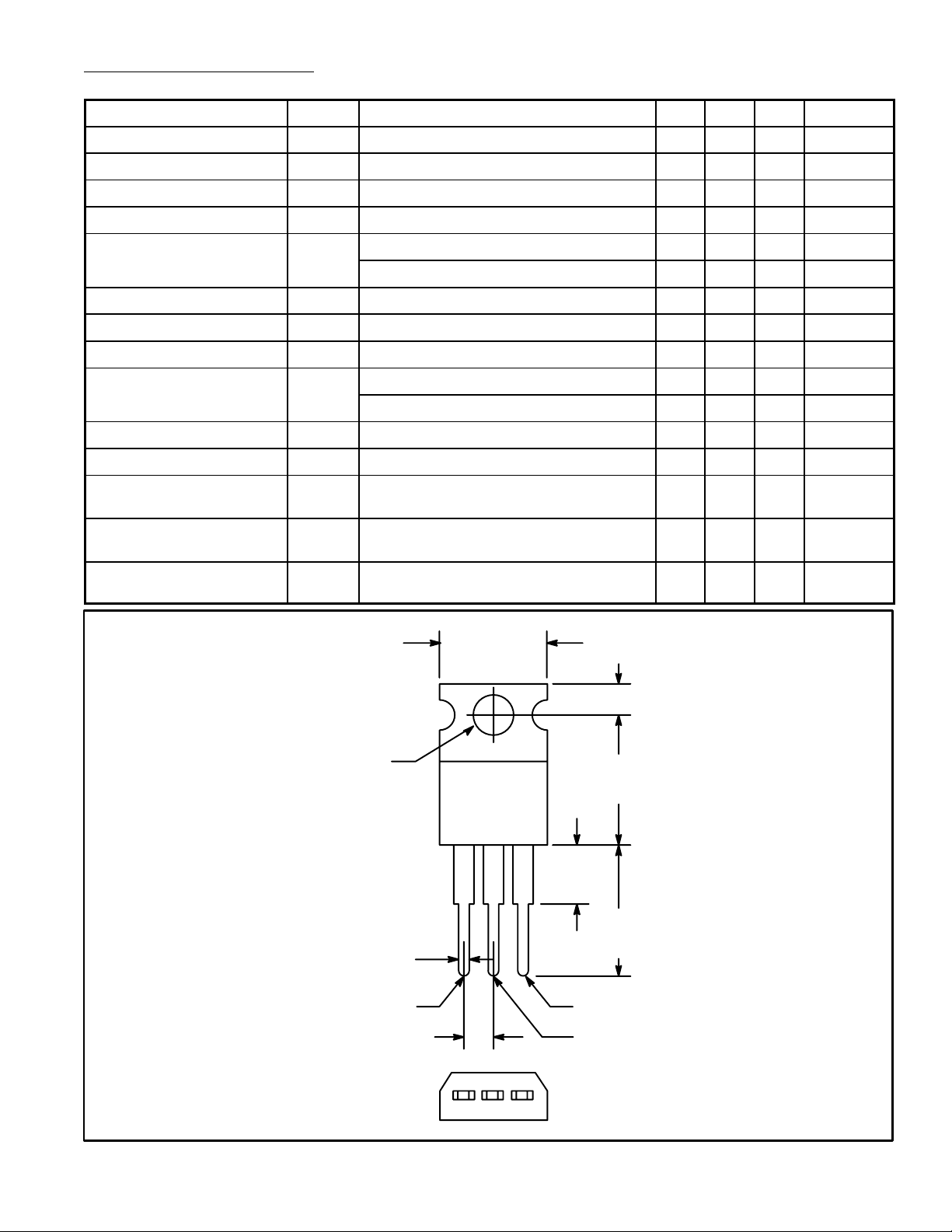
.147
(3.75)
Dia
Max
.070 (1.78) Max
V
.100 (2.54)
.420 (10.67)
Max
.110 (2.79)
GND
.500
(12.7)
Max
.250 (6.35)
Max
.500
(12.7)
Min
IN
V
OUT
GND
 Loading...