

NTE NTE1934 Datasheet
NTE1934
Integrated Circuit
Positive Voltage Regulator,
5V, 2A
Features:
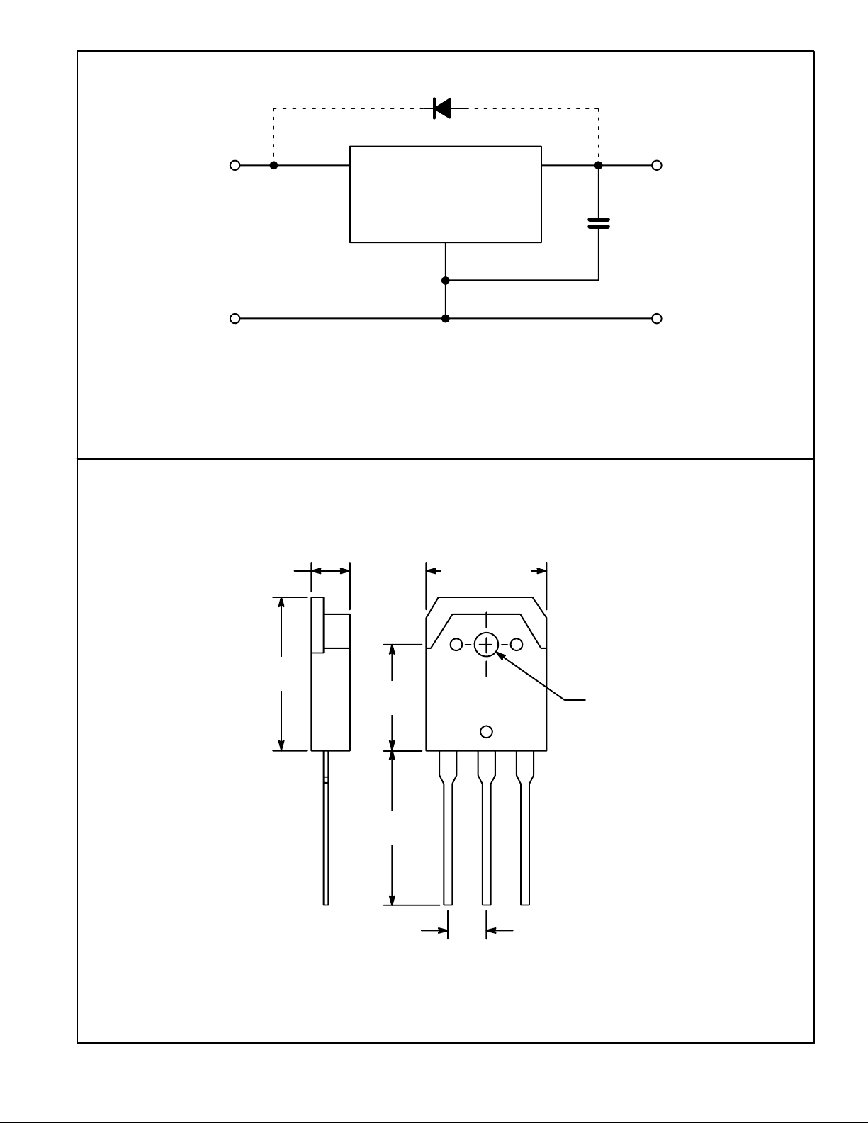
D 3 Pin Plastic Package TO3P
D Precise Setting Voltage of ±2%
D Wide Input Voltage Range (∼45V)
D Built–in Current Foldback Protection
D Ideal Combination of Passivated Power Transistor and High Reliability Flip–Chip Circuit
Absolute Maximum Ratings:
DC Input Voltage, V
Power Dissipation, P
IN
C(TC
(TA = +25°C unless otherwise specified)
=+ 25°C) 50W. . . . . . . . . . . . . . . . . . . . . . . . . . . . . . . . . . . . . . . . . . . . . . . . .
(No Fin) 2W. . . . . . . . . . . . . . . . . . . . . . . . . . . . . . . . . . . . . . . . . . . . . . . . . . . . . .
Thermal Resistance, Junction–to–Case, R
Junction Temperature Range, T
j
Operating Ambient Temperature Range, T
Storage Temperature Range, T
Electrical Characteristics:
stg
(TA = +25°C unless otherwise specified)
thJC
op
Parameter Symbol Test Conditions Min Typ Max Unit
DC Input Voltage V
Output Voltage V
Output Current I
Line Regulation ∆V
Load Regulation ∆V
Temperature Coefficient K
IN
O
O
LINE
LOADVIN
IO = 2A 8 – 30 V
VIN = 10V, IO = 0.5A 4.9 5.0 5.1 V
VIN = 8.5V to 11.5V, IO = 0.5A – 2 10 mV
= 10V, IO = 0 to 2A – 40 100 mV
t
Ripple Rejection 100 to 120H
Foldback Current I
Short–Circuit Current I
S1
S2
45V. . . . . . . . . . . . . . . . . . . . . . . . . . . . . . . . . . . . . . . . . . . . . . . . . . . . . . . . . . . . . . .
2°C/W. . . . . . . . . . . . . . . . . . . . . . . . . . . . . . . . . . . . . . .
–30° to +125°C. . . . . . . . . . . . . . . . . . . . . . . . . . . . . . . . . . . . . . . . . . . .
–20° to +80°C. . . . . . . . . . . . . . . . . . . . . . . . . . . . . . . . . .
–30° to +125°C. . . . . . . . . . . . . . . . . . . . . . . . . . . . . . . . . . . . . . . . . .
0 – 2 A
– ±0.5 – mV/°C
Z
– 60 – dB
2.4 – – A
– – 0.6 A
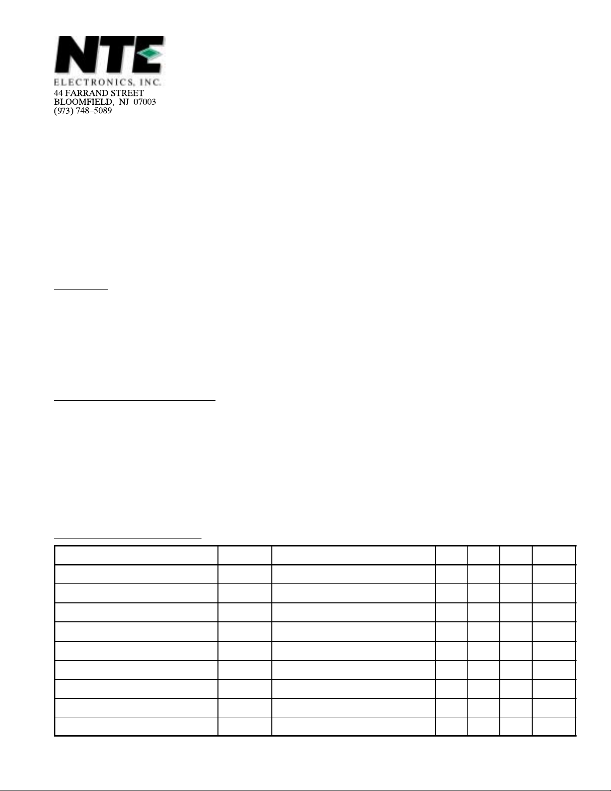
External Circuit
D
1
21
+
V
IN
DC Input
3
C
1
V
–
O
DC Output
Note 1. Output capacitor C1 (47 to 100µf) shall be connected directly to output terminal (Pin1)
and GND terminal (PIn3) as shown above.
Note 2. When wiring between the regulator and the load is long, another capacitor (47 to 100µf)
shall be added in parallel with the load.
Note 3. If there is a possibility of reverse biasing between input and output, a protection diode
(D
) is to be added. The recommended diode for D1 is NTE116.
1
.787
(20.0)
.591
(15.02)
.787
(20.0)
.615 (15.62).190 (4.82)
V
IN
.126 (3.22)
Dia
V
V
O
IN
GND
.215 (5.47)
 Loading...