

NTE NTE1912 Datasheet

NTE1912
Integrated Circuit
Positive 3 Terminal Voltage Regulator,
12V, 3A
Description:
The NTE1912 is a 3 terminal fixed positive voltage regulator in a TO3 type package designed for use
in applications r equiring a w ell regulated positive o utput v oltage. Outstanding f eatures i nclude f ull power
usage up to 3A o f l oad c urrent, i nternal current limiting, thermal shutdown, and safe a rea p rotection o n
the chip, providing protection o f t he s eries p ass D arlington, u nder m ost o perating c onditions. Hermetically sealed s teel p ackages a re u tilized f or h igh r eliability a nd low thermal r esistance. A low–noise temperature stable band–gap reference is the key design factor insuring excellent temperature regulation
of the NTE1912. This coupled to a very low output impedance insures superior load regulation.
Features:
D Guaranteed Power Dissipation: PD = 30W @ TC = 57.5°C
D Guaranteed Input–Output Differential: V
D Low Noise, Band Gap Reference
D Remote Sense Capability
D Sample Power Cycled Burn–In
D Guaranteed Thermal Resistance Junction to Case: R
– VO = +2.5V
IN
= 2.25°C/W
Θ
JC
Absolute Maximum Ratings:
Input Voltage (Note 1), V
Power Dissipation, P
Derate Above T
Operating Junction Temperature Range, T
Storage Temperature Range, T
IN
D
= 57.5°C 444mW/°C. . . . . . . . . . . . . . . . . . . . . . . . . . . . . . . . . . . . . . . . . . . . . .
C
J
stg
Lead Temperature (During Soldering, 60sec Max), T
Thermal Resistance, Junction to Case, R
Θ
JC
Note 1. Short circuit protection is only assured to V
voltages approaching V
max, regulator may require the removal of the input voltage to re-
IN
start.
Internally Limited. . . . . . . . . . . . . . . . . . . . . . . . . . . . . . . . . . . . . . . . . . . . . . . . . .
–55° to +150°C. . . . . . . . . . . . . . . . . . . . . . . . . . . . . . . . . .
–65° to +150°C. . . . . . . . . . . . . . . . . . . . . . . . . . . . . . . . . . . . . . . . . .
L
+300°C. . . . . . . . . . . . . . . . . . . . . . . . . . . . . . . .
2.25°C/W. . . . . . . . . . . . . . . . . . . . . . . . . . . . . . . . . . . . . .
max. In case of short circuit, with input–output
IN
30V. . . . . . . . . . . . . . . . . . . . . . . . . . . . . . . . . . . . . . . . . . . . . . . . . . . . . . . . . .
Electrical Characteristics: (TJ = +25°C unless otherwise specified)
Parameter Symbol Test Conditions Min Typ Max Unit
Output Voltage V
Input–Output Differential VIN–VOIO = 3A, TJ = 0 to +125°C 2.5 – – V
Line Regulation Reg
Load Regulation Reg
Quiescent Current I
Quiescent Current Line I
Quiescent Current Load I
Current Limit I
Temperature Coefficient T
Output Noise Voltage V
Ripple Attenuation R
Power Dissipation P
Q(Line)VIN
Q(Load)VIN
LIM
VIN = 15V to 22V, IO = 10mA to 3A, Note 2 11.05 12.0 13.05 V
O
LineVIN
LoadVIN
Q
C
N
A
D
= 15V to 27V, IO = 2A, Note 2 – – 1.0 % V
= 17V, IO = 10mA to 3A, Note 2 – – 0.6 % V
VIN = 15V, IO = 10mA – – 20 mA
= 15V to 22V, IO = 10mA – – 5 mA
= 15V, IO = 10mA to 3A – – 5 mA
VIN = 17V, Note 2 – – 6.5 A
VIN = 15V, IO = 100mA, TJ = 0 to +125°C – – 0.02 % VO/°C
VIN = 15V, IO = 100mA. TJ = 0 to +125°C, Note 3 – – 10 µV
VIN = 17V, IO = 2A, TJ = 0 to +125°C, Note 4 60 – – dB
VIN – VO (2.5V to 10V), IO = 10mA to 3A,
= 0 to +125°C
T
J
– – 30 W
rms
O
O
/V
Note 2. Low duty cycle pulse testing with Kelvin connections required. Die temperature changes
must be accounted for separatly.
Note 3. BW = 10Hz to 100kHz.
Note 4. Ripple attenuation is specified for a 1Vrms, 120Hz, input ripple. Ripple attenuation is mini-
mum of 60dB at 5V output and is 1dB less for each volt increase in the output voltage.
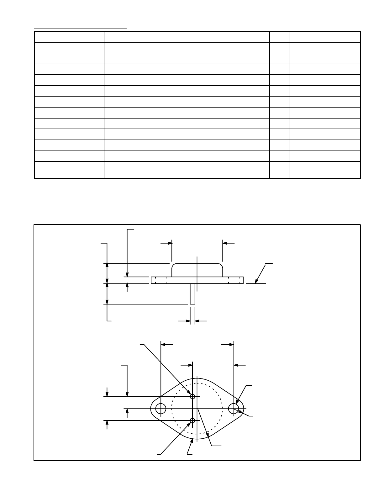
.350 (8.89)
.215 (5.45)
.430
(10.92)
.135 (3.45) Max
V
OUT
.875 (22.2)
Dia Max
Seating
Plane
.040 (1.02).312 (7.93) Min
1.187 (30.16)
.665
(16.9)
.156 (3.96) Dia
(2 Holes)
.188 (4.8) R Max
IN
.525 (13.35) R Max
Common/CaseV
 Loading...