

NTE NTE1910 Datasheet
NTE1910
Integrated Circuit
Positive 3 Terminal Voltage Regulator,
9V, 1A
Description:
The NTE1910 is a 3 t erminal fixed positive voltage r egulator i n a TO220 type package. S tabilized f ixed
output voltage is obtained from unstabe DC input voltage without the use of external components.
Features:
D No External Components
D Output Current in Excess of 1A
D Internal Short–Circuit Current Limiting
D Internal Thermal Overload Protection
D Output Transistor Safe Area Compensation
Absolute Maximum Ratings:
Input Voltage, V
Power Dissipation, P
I
D
(TA = 25°C unless otherwise specified)
Operating Ambient Temperature Range, T
Storage Temperature Range, T
Electrical Characteristics:
Parameter Symbol Test Conditions Min Typ Max Unit
Output Voltage V
Output Voltage Tolerance V
Line Regulation REG
Load Regulation REG
Bias Current I
Input Bias Current Change ∆I
stg
(TA = +25°C unless otherwise specified)
O
O
BIAS
BIAS(IN)VI
TJ = 25°C 8.65 9.0 9.35 V
VI = 12V to 24V, IO = 5mA to1A,
T
J
VI = 11.5V to 26V, TJ = 25°C – 7 180 mV
IN
VI = 12V to 18V, TJ = 25°C – 2 90 mV
LIO
IO = 250mA to 750mA, TJ = 25°C – 4 90 mV
TJ = 25°C – 3.9 8.0 mA
15W. . . . . . . . . . . . . . . . . . . . . . . . . . . . . . . . . . . . . . . . . . . . . . . . . . . . . . . . . . . . .
opr
–30° to +80C. . . . . . . . . . . . . . . . . . . . . . . . . . . . . . . . . . .
–55° to +150C. . . . . . . . . . . . . . . . . . . . . . . . . . . . . . . . . . . . . . . . . .
8.55 – 9.45 V
= 0° to +125°C, PD ≤ 15W
= 5mA to 1.5A, TJ = 25°C – 12 180 mV
= 11.5V to 26V, TJ = 25°C – – 1 mA
35V. . . . . . . . . . . . . . . . . . . . . . . . . . . . . . . . . . . . . . . . . . . . . . . . . . . . . . . . . . . . . . . . . . .
Electrical Characteristics (Cont’d): (TA = +25°C unless otherwise specified)
Parameter Symbol Test Conditions Min Typ Max Unit
Load Bias Current Change ∆I
Output Noise Voltage V
BIAS(L)IO
no
Ripple Rejection Ratio RR VI = 12V to 22V, IO = 100mA,
= 5mA to 1.5A, TJ = 25°C – – 0.5 mA
f = 10Hz to 100kHz – 57 – µV
56 – – dB
f = 120Hz
Minimum Input/Output
V
DIF(min)IO
= 1A, TJ = 25°C – 2 – V
Voltage Difference
Output Impedance Z
Output Short Circuit Current I
Peak Output Current I
Output Voltage Temperature
O(short)
O(peak)
∆VO/TAIO = 5mA, TJ = 0° to +125°C – –0.5 – mV/°C
O
f = 1kHz – 16 –
mΩ
VI = 26V, TJ = 25°C – 700 – mA
TJ = 25°C – 2 – A
Coefficient
Note 1. The specified condition, TJ = +25°C, means that the test should be carried out with the test
time so short (within 10ms) that the drift in characteristic value due to the rise in chip junction
temperature can be ignored.
Note 2. When not specified, V
= 15V, IO = 500mA, CI = 0.33µf, and CO = 0.1µf.
I
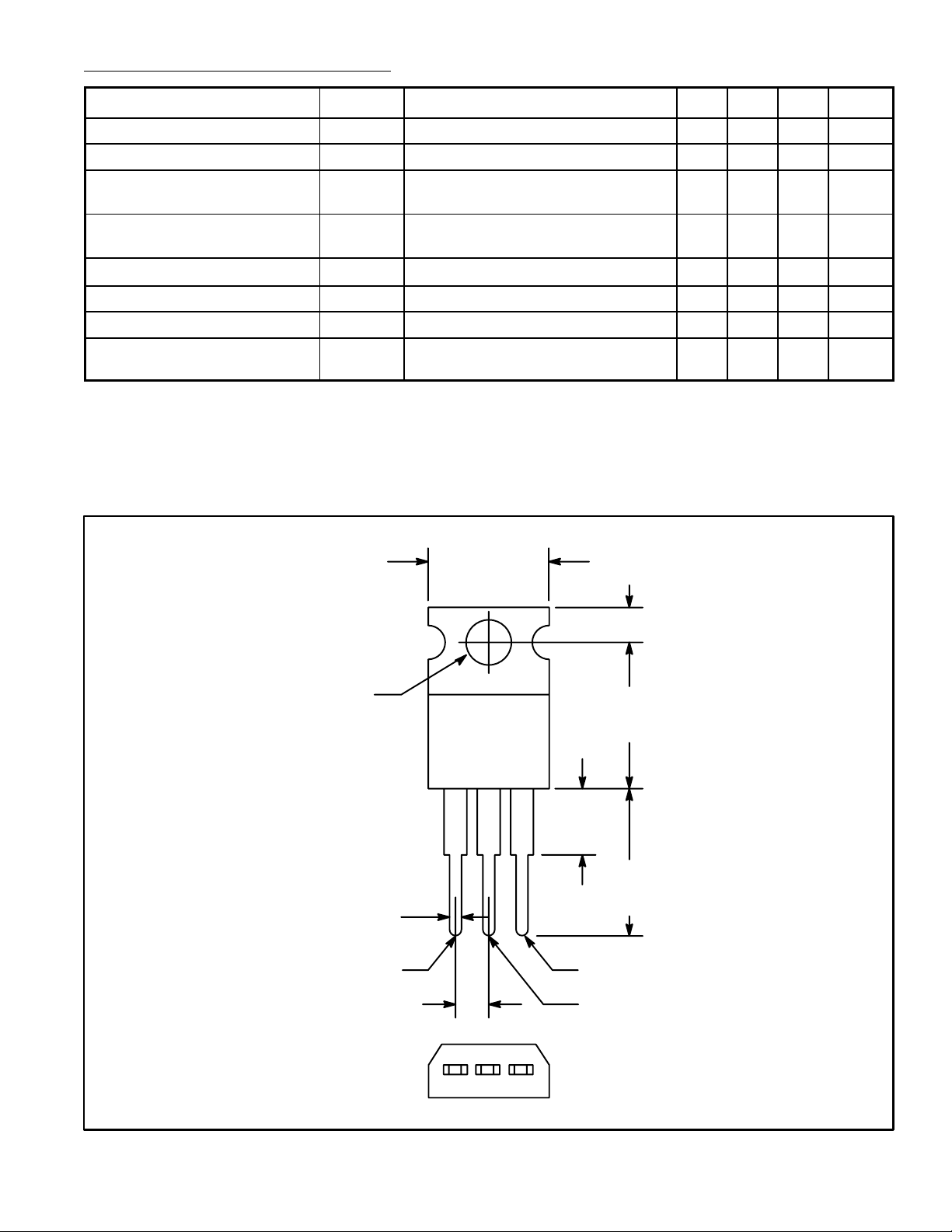
.420 (10.67)
Max
.147 (3.75)
Dia Max
.070 (1.78)
Max
.100 (2.54)
.110 (2.79)
.500
(12.7)
Max
.250 (6.35)
Max
.500
(12.7)
Min
V
IN
V
OUT
GND/Tab
 Loading...