

NTE NTE1906 Datasheet
NTE1906
Integrated Circuit
Positive 3 Terminal Voltage Regulator,
18V, 100mA
Description:
The NTE1906 is a positive 3–terminal voltage regulator in a TO92 type package suitable for numerous
applications requiring up to 100mA. This device features thermal shutdown and current limiting making
the NTE1906 remarkably rugged. In most applications, no external components are required.
The NTE1906 is useful for on–card regulation or any other application where a regulated positive voltage at a modest current level is needed. This device offers a substantial advantage over he common
resistor/zener diode approach.
Features:
D Internal Short–Circuit Current Limiting
D Internal Thermal Overload Protection
D No External Components Required
Absolute Maximum Ratings:
Input Voltage, V
Internal Power Dissipation (Note 1), P
Operating Junction Temperature Range, T
Maximum Junction Temperature, T
Storage Junction Temperature Range, T
I
D
opr
J
stg
Lead Temperature (During Soldring, 10sec), T
Internally Limited. . . . . . . . . . . . . . . . . . . . . . . . . . . . . . . . . . .
0° to +70°C. . . . . . . . . . . . . . . . . . . . . . . . . . . . . . . . . . .
–55° to +150°C. . . . . . . . . . . . . . . . . . . . . . . . . . . . . . . . . .
L
35V. . . . . . . . . . . . . . . . . . . . . . . . . . . . . . . . . . . . . . . . . . . . . . . . . . . . . . . . . . . . . . . . . . .
+125°C. . . . . . . . . . . . . . . . . . . . . . . . . . . . . . . . . . . . . . . . . . . . . . .
+300°C. . . . . . . . . . . . . . . . . . . . . . . . . . . . . . . . . . . . .
Note 1. Thermal resistance, junction–to–ambient is 180°C/W when mounted with 0.4” leads on a PC
board and 160°C/W when mounted with .250” leads on a PC board.
Electrical Characteristics:
(VI = 27V, IO = 40mA, CI = 0.33µF, CO = 0.1µF, 0° < TJ < +125°C
unless otherwise specified)
Parameter Symbol Test Conditions Min Typ Max Unit
Output Voltage V
Line Regulation Reg
TJ = +25°C 17.3 18.0 18.7 V
O
20.7V ≤ VI ≤ 33V, 1mA ≤ IO ≤ 100mA 17.1 18.0 18.9 V
lineTJ
= +25°C, 20.7V ≤ VI ≤ 33V – – 325 mV
Electrical Characteristics (Cont’d): (VI = 27V, IO = 40mA, CI = 0.33µF, CO = 0.1µF,
0° < T
Parameter Symbol Test Conditions Min Typ Max Unit
< +125°C unless otherwise specified)
J
Load Regulation Reg
Quiescent Current I
Quiescent Current Change ∆I
Output Noise Voltage V
Long–Term Stability ∆VO/∆t – 56 – mV/1kHrs
Ripple Rejection RR f = 120Hz, 23V ≤ VI ≤ 33V 33 48 – dB
Dropout Voltage V
loadTJ
B
B
n
DO
= +25°C, 1mA ≤ IO ≤ 100mA – – 170 mV
TJ = +125°C – 2 6 mA
With line, 21V ≤ VI ≤ 33V – – 1.5 mA
With load, 1mA ≤ IO ≤ 40mA – – 0.1 mA
TJ = +25°C, f = 10Hz to 10kHz – 150 – µV
TJ = +25°C, IO = 40mA – 1.7 – V
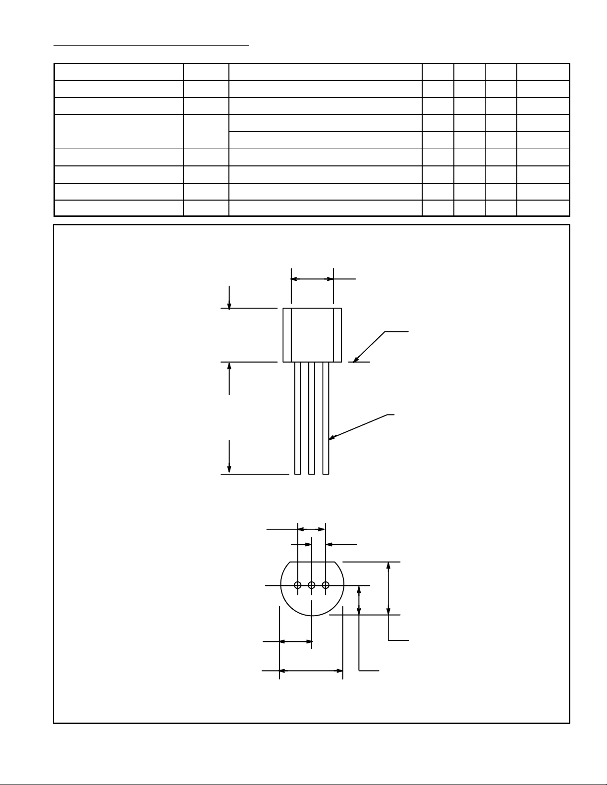
.135 (3.45) Min
.210
(5.33)
Seating Plane
Max
.500
(12.7)
Min
.100 (2.54)
.105 (2.67) Max
.205 (5.2) Max
V
OUT
GND
V
.021 (.445) Dia Max
IN
.050 (1.27)
.165 (4.2) Max
.105 (2.67) Max
 Loading...