NTE NTE1905 Datasheet

NTE1905
Integrated Circuit
Negative 3 Terminal Voltage Regulator,
–15V, 100mA
Description:
The NTE1905 voltage regulator is an inexpensive, easy–to–use device in a TO92 type p ackage s uitable
for a multitude o f a pplications t hat r equire a r egulated s upply o f u p to 100mA. T his d evice f eatures internal current limiting a nd t hermal s hutdown m aking t he N TE1905 r emarkably r ugged. No external components are required in many applications.
The NTE1905 offers a substantial performance advantage over the traditional zener diode–resistor
combination, as output impedance and quiescent current are substantially reduced.
Features:
D Low Cost
D ±5% Tolerance
D Internal Short–Circuit Current Limiting
D Internal Thermal Overload Protection
D No External Components Required
Absolute Maximum Ratings:
Input Voltage, V
I
Operating Junction Temperature Range, T
Storage Junction Temperature Range, T
Electrical Characteristics:
(TA = +25°C unless otherwise specified)
J
stg
(VI = –33V, IO = 40mA, CI = 0.33µF, CO = 0.1µF, 0° < TJ < +125°C
unless otherwise specified)
Parameter Symbol Test Conditions Min Typ Max Unit
Output Voltage V
Line Regulation Reg
TJ = +25°C –14.4 –15 –15.6 V
O
–17.5V ≥ VI ≥ –30V, 1.0mA ≤ IO ≤ 40mA –14.25 – –15.75 V
VI = –23V, 1.0mA ≤ IO ≤ 70mA –14.25 – –15.75 V
line
TJ = +25°C
–17.5V ≥ VI ≥ –30V – – 300 mV
–20V ≥ VI ≥ –30V – – 250 mV
–35V. . . . . . . . . . . . . . . . . . . . . . . . . . . . . . . . . . . . . . . . . . . . . . . . . . . . . . . . . . . . . . . . . .
0° to +150°C. . . . . . . . . . . . . . . . . . . . . . . . . . . . . . . . . . . .
–65° to +150°C. . . . . . . . . . . . . . . . . . . . . . . . . . . . . . . . . .

Electrical Characteristics (Cont’d): (VI = –33V, IO = 40mA, CI = 0.33µF, CO = 0.1µF,
0° < T
Parameter Symbol Test Conditions Min Typ Max Unit
< +125°C unless otherwise specified)
J
Load Regulation Reg
Input Bias Current I
Input Bias Current
Change
Output Noise Voltage V
Long–Term Stability ∆VO/∆t – 30 – mV/1.0kHrs
Ripple Rejection RR –18.5V ≤ VI ≤ –28.5V, f = 120Hz 34 39 – dB
Input–Output Voltage
Differential
loadTJ
IB
∆I
IB
n
|VI/VO| IO = 40mA, TJ = +25°C – 1.7 – V
= +25°C 1.0mA ≤ IO ≤ 100mA – – 150 mV
1.0mA ≤ IO ≤ 40mA – – 75 mV
TJ = +25°C – – 6.5 mA
TJ = +125°C – – 6.0 mA
–20V ≥ VI ≥ –30V – – 1.5 mA
1.0mA ≤ IO ≤ 40mA – – 0.1 mA
TA = +25°C, 10Hz ≤ f ≤ 100kHz – 90 – µV
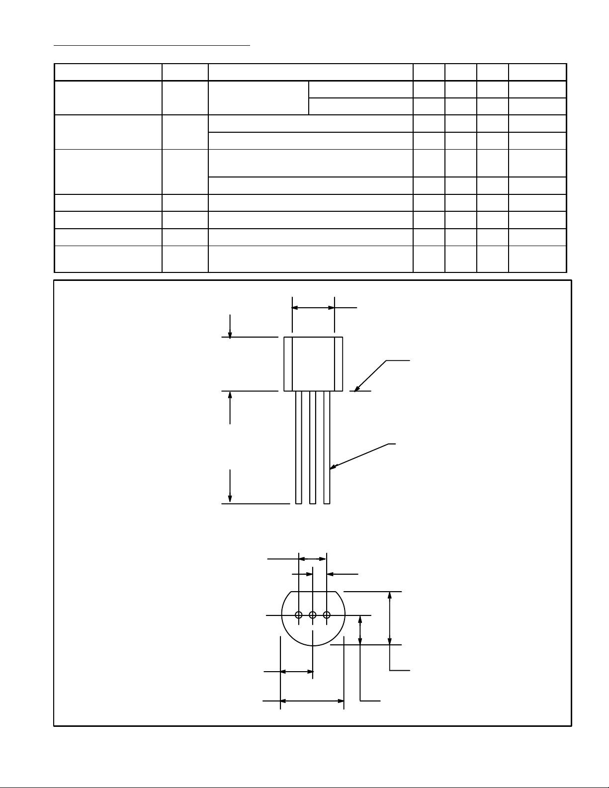
.135 (3.45) Min
.210
(5.33)
Seating Plane
Max
.500
(12.7)
Min
.100 (2.54)
.105 (2.67) Max
.205 (5.2) Max
GND
V
IN
V
OUT
.021 (.445) Dia Max
.050 (1.27)
.165 (4.2) Max
.105 (2.67) Max
 Loading...