

NTE NTE1900 Datasheet

NTE1900
Integrated Circuit
3–Terminal Adjustable Positive
Voltage Regulator
Description:
The NTE1900 is an adjustable 3–terminal positive voltage regulator in a TO92 type package capable
of supplying in excess of 100mA over a 1.2V to 37V output range. This device is exceptionally easy
to use and both line and load regulation are better than standard fixed regulators.
In addition to higher performance than fixed regulators, the NTE1900 offers full overload protection
available only in IC’s. Included on the chip are current limit, thermal overload protection, and safe
area protection. All overload protection circuitry remains fully functional even if the adjustment terminal is disconnected.
Normally, no capacitors are needed unless the device is situated far from the input filter capacitors
in which case an input bypass is needed. An optional output capacitor can be added to improve transient response. The adjustment terminal can be bypassed to achieve very high ripple rejection ratios
which are difficult to achieve with standard 3–terminal regulators.
Besides replacing fixed r egulators, t he N TE1900 i s u seful i n a wide variety of other a pplications. Since
the regulator is “floating” and sees only the input–to–output differential voltage, supplies of several
hundred volts can be regulated as long as the maximum input to output differential is not exceeded.
Also, it makes an especially simple adjustable switching regulator, a programmable output regulator,
or by connecting a fixed resistor between the adjustment and output, the NTE1900 can be used as
a precision current regulator. Supplies with electronic shutdown can be achieved by clamping the
adjustment terminal to GND which programs the output to 1.2V where most loads draw little current.
Features:
D Adjustable Output Down to 1.2V
D Guaranteed 100mA Output Current
D Line Regulation Typically 0.01%/V
D Load Regulation Typically 0.1%
D Current Limit Constant with Temperature
D Eliminates the Need to Stock Many Voltages
D 80dB Ripple Rejection
Absolute Maximum Ratings:
Power Dissipation, P
Input–Output Voltage Differential, V
Operating Junction Temperature Range, T
Storage Temperature Range, T
Lead Temperature (During Soldering, 10sec), T
D
I–VO
J
stg
L
Internally Limited. . . . . . . . . . . . . . . . . . . . . . . . . . . . . . . . . . . . . . . . . . . . . . . . . .
40V. . . . . . . . . . . . . . . . . . . . . . . . . . . . . . . . . . . . . . . . . . . . . . .
–40° to +125°C. . . . . . . . . . . . . . . . . . . . . . . . . . . . . . . . . .
–65° to +150°C. . . . . . . . . . . . . . . . . . . . . . . . . . . . . . . . . . . . . . . . . .
+300°C. . . . . . . . . . . . . . . . . . . . . . . . . . . . . . . . . . . .
Electrical Characteristics: (–25° ≤ TJ ≤ +125°C, VIN–V
= 5V, IO = 40mA, I
OUT
= 100mA,
MAX
Note 1 unless otherwise specified)
Parameter Symbol Test Conditions Min Typ Max Unit
Line Regulation Reg
Load Regulation Reg
lineTA
loadTA
Thermal Regulation TA = +25°C, 10ms Pulse – 0.04 0.2 %/W
Adjustment Pin Current I
Adjustment Pin Current
∆I
Adj
Adj
Change
Reference Voltage V
Temperature Stability T
Minimum Load Current I
Maximum Output Current I
ref
S
Lmin
max
Limit
RMS Output Noise,
% of V
OUT
N TA = +25°C, 10Hz ≤ f ≤ 10kHz – 0.003 – %
Ripple Rejection Ratio RR V
Long Term Stability S TJ = +125°C, 1000 Hours – 0.3 1.0 %
= +25°C, 3V ≤ (VIN–V
3V ≤ (VIN–V
) ≤ 40V – 0.02 0.07 %/V
OUT
= +25°C, 5mA ≤ IO ≤ 1
) ≤ 40V, Note 2 – 0.01 0.04 %/V
OUT
, Note 2 – 0.1 0.5 %
MAX
5mA ≤ IO ≤ 100mA, Note 2 – 0.3 1.5 %
– 50 100 µA
5mA ≤ IL ≤ 100mA, 3V ≤ (VIN–V
OUT
) ≤ 40V,
– 0.2 5.0 µA
P ≤ 625mW
3V ≤ (VIN–V
) ≤ 40V, 5mA ≤ IO ≤ 100mA,
OUT
1.20 1.25 1.30 V
P ≤ 625mW, Note 3
–25° ≤ TJ ≤ +125°C – 0.65 – %
(VIN–V
3V ≤ (VIN–V
3V ≤ (VIN–V
VIN–V
OUT
C
ADJ
) ≤ 40V – 3.5 5 mA
OUT
) ≤ 15V – 1.5 2.5 mA
OUT
) ≤ 13V 100 200 300 mA
OUT
= 40V 25 50 150 mA
OUT
= 10V, f = 120Hz, C
= 0 – 65 – dB
ADJ
= 10µF 66 80 – dB
Note 1. Although power dissipation is internally limited, these specifications are applicable for power
dissipations of 625mW.
Note 2. Regulation is measured at constant junction temperature, using pulse testing with a low duty
cycle. Changes in output voltage due to heating effects are covered under the specification
for thermal regulation.
Note 3. Thermal resistance is 180°C/W junction to ambient with 0.4” leads from a PC board and
160°C/W junction to ambient with 0.125” lead length to PC board.
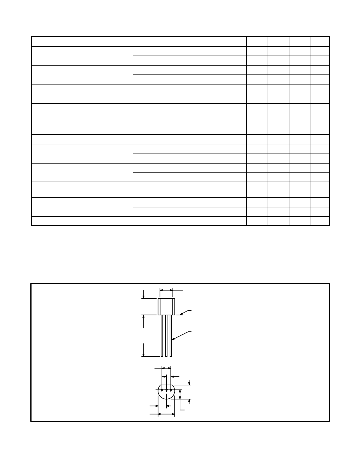
.135 (3.45) Min
.210
(5.33)
Max
.500
(12.7)
Min
.100 (2.54)
Adj
V
OUT
V
IN
Seating Plane
.021 (.445) Dia Max
.050 (1.27)
.165
(4.2)
Max
.105 (2.67) Max
.205 (5.2) Max
.105 (2.67) Max
 Loading...