

NTE NTE1899, NTE1898 Datasheet

NTE1898 & NTE1899
Integrated Circuit
Dual Audio Power Amp, 5.8W (22W BTL)
Description:
The NTE1898 and NTE1899 are dual audio power amplifiers in a 12–Lead SIP type package designed for use as high performance, car–audio power amplifiers in consumer applications. These
devices feature high power, low distortion, and low noise along with various types of protection circuits. The NTE1899 is a mirror image pin–out of the NTE1898 allowing for easier design of PC boards
when used in BTL–stereo applications.
Features:
D High Power:
P
= 22W (Typ) @ VCC = 14.4V, f = 1kHz, THD = 10%, RL = 4Ω (BTL)
OUT
= 5.8W/Ch (Typ) @ VCC = 13.2V, f = 1kHz, THD = 10%, RL = 4Ω (Dual)
P
OUT
D Low Distortion:
THD = 0.03% (Typ) @ V
THD = 0.06% (Typ) @ V
D Low Noise:
V
= 0.14mV
NO
= 0.7mV
V
NO
D Protector Circuit:
Thermal Shut Down, Overvoltage, OUT–V
(Typ) @ VCC = 13.2V, RL = 4Ω, GV = 40dB, Rg = 0, DIN Noise: DIN45405
rms
(Typ) @ VCC = 13.2V, RL = 4Ω, GV = 52dB, BW = 20Hz to 20kHz (Dual)
rms
= 14.4V, f = 1kHz, P
CC
= 13.2V, f = 1kHz, P
CC
= 4W, RL = 4Ω, GV = 40dB (BTL)
OUT
= 1W, RL = 4Ω, GV = 52dB (Dual)
OUT
Short, OUT–GND Short, OUT–OUT Short
CC
Absolute Maximum Ratings:
(TA = +25°C unless othrwise specified)
Peak Supply Voltage (0.2sec), V
DC Supply Voltage, V
Operating Supply Voltage, V
Peak Output Current, I
Power Dissipation, P
DC 25V. . . . . . . . . . . . . . . . . . . . . . . . . . . . . . . . . . . . . . . . . . . . . . . . . . . . . . . . . .
CC
opr 18V. . . . . . . . . . . . . . . . . . . . . . . . . . . . . . . . . . . . . . . . . . . . . . . . . . . .
CC
peak 4.5A. . . . . . . . . . . . . . . . . . . . . . . . . . . . . . . . . . . . . . . . . . . . . . . . . . . . . . .
O
D
Operating Temperature Range, T
Storage Temperature Range, T
stg
surge 45V. . . . . . . . . . . . . . . . . . . . . . . . . . . . . . . . . . . . . . . . . . . . . .
CC
opr
–30° to +85°C. . . . . . . . . . . . . . . . . . . . . . . . . . . . . . . . . . . . . . . . .
–55° to +150°C. . . . . . . . . . . . . . . . . . . . . . . . . . . . . . . . . . . . . . . . . .
25W. . . . . . . . . . . . . . . . . . . . . . . . . . . . . . . . . . . . . . . . . . . . . . . . . . . . . . . . . . . . .
Electrical Characteristics: (TA = +25°C, VCC = 13.2V, RL = 4Ω, Rg = 600Ω, f = 1kHz unless
othrwise specified)
Parameter Symbol Test Conditions Min Typ Max Unit
Quiescent Current I
BTL Connection Mode
Output Power P
Total Harmonic Distortion THD P
Output Offset Voltage V
Voltage Gain G
Output Noise Voltage V
Ripple Rejection Ratio RR f
Dual Mode
Output Power P
Total Harmonic Distortion THD P
Voltage Gain G
Voltage Gain Ratio ∆G
Output Noise Voltage V
Ripple Rejection Ratio RR f
Crosstalk CT V
Input Resistance R
CCQ
OUT
OFF
V
NO
OUT
V
V
NO
IN
VIN = 0 – 80 145 mA
VCC = 14.4V, THD = 10% – 22 – W
THD = 10% 16 19 – W
THD = 1% 12 15 – W
= 4W, GV = 40dB – 0.03 0.25 %
OUT
VIN = 0 – 0 0.35 V
V
= 0dBm – 40 – dB
OUT
Rg = 0, DIN 45405 Noise Filter – 0.14 – mV
= 100Hz, V
ripple
THD = 10% 5.0 5.8 – W
= 1W – 0.06 0.30 %
OUT
V
= 0dBm 50 52 54 dB
OUT
V
= 0dBm –1 – +1 dB
OUT
Rg = 10kΩ, BW = 20Hz to 20kHz – 0.7 1.5 mV
= 100Hz, V
ripple
= 0dBm – –57 – dB
OUT
f = 1kHz – 33 – kΩ
= 0dBm – –52 –40 dB
ripple
= 0dBm – –52 –40 dB
ripple
rms
rms
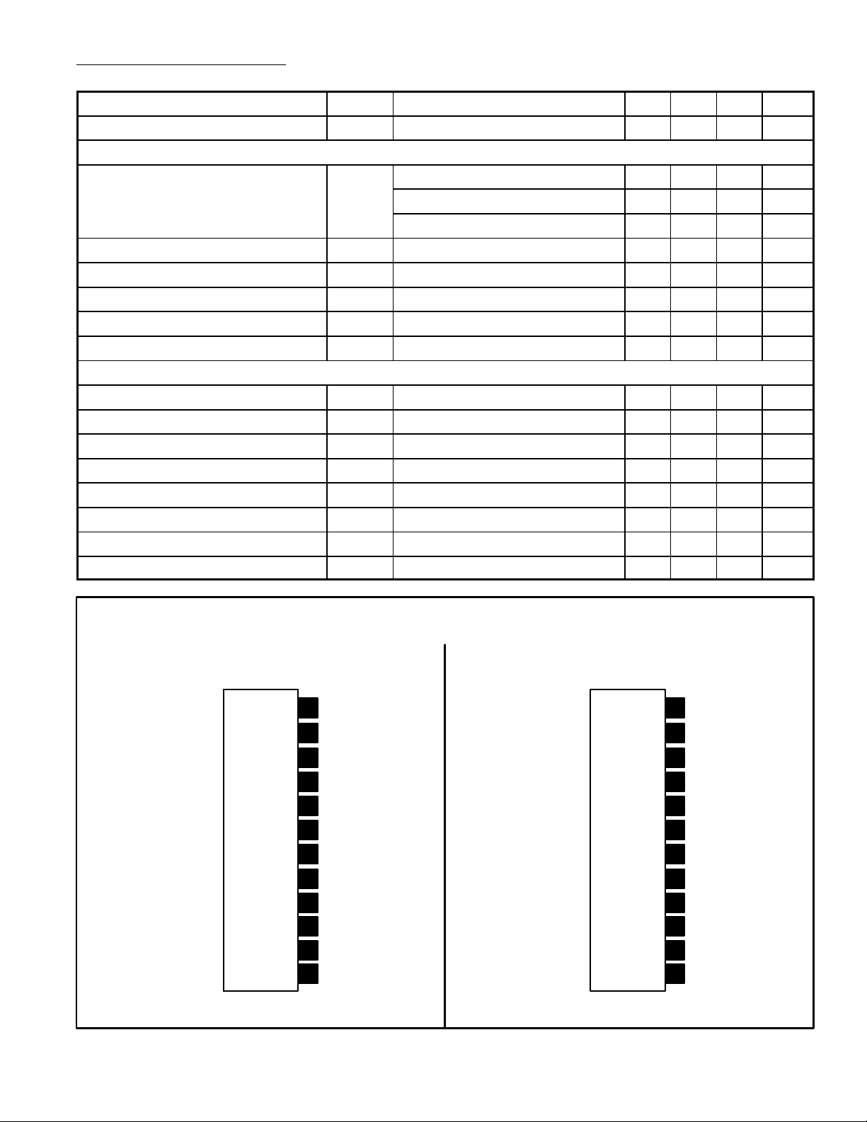
Pin Connection Diagram
(Front View)
NTE1898 NTE1899
Output 1
12
Bootstrap 1
11
10
V
CC
Power GND
9
Bootstrap 2
8
Output 2
7
Ripple
6
Input 2
5
4
NF 2
Pre GND
3
NF 1
2
Input 1
1
Input 1
12
NF 1
11
10
Pre GND
NF 2
9
Input 2
8
Ripple
7
Output 2
6
Bootstrap 2
5
4
Power GND
3
V
CC
Bootstrap 1
2
Output 1
1
 Loading...