

NTE1890
Integrated Circuit
NTSC Decoder for TV
Description:
The NTE1890 is a monolithic integrated decoder for the NTSC color television standards. It combines
all functions required for the demodulation of NTSC signals. Further more it contains a luminance
amplifier, an RGB–matrix and amplifier. These amplifiers supply output signals up to 5V peak–to–
peak (picture information) enabling direct drive of the discrete output stages.
Absolute Maximum Ratings:
Maximum Supply Voltage (Pin1), VP = V
Maximum Total Power Disipation, P
Operating Ambient Temperature Range, T
Storage Temperature Range, T
stg
1–23
tot
A
Thermal Resistance, Junction–to–Ambient, R
–25° to +65°C. . . . . . . . . . . . . . . . . . . . . . . . . . . . . . . . . . .
–25° to +150°C. . . . . . . . . . . . . . . . . . . . . . . . . . . . . . . . . . . . . . . . . .
thJA
13.2V. . . . . . . . . . . . . . . . . . . . . . . . . . . . . . . . . . . . . . . . .
1.7W. . . . . . . . . . . . . . . . . . . . . . . . . . . . . . . . . . . . . . . . . . . . . . . .
50K/W. . . . . . . . . . . . . . . . . . . . . . . . . . . . . . . . . . . .
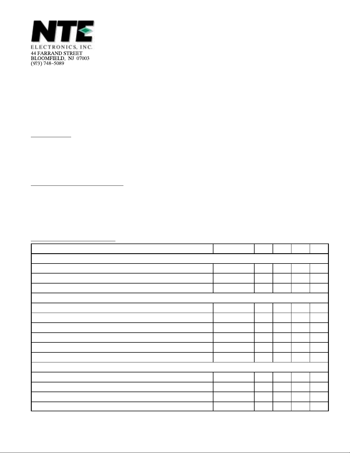
Electrical Characteristics:
Supply (Pin1)
Supply Voltage VP = V
Supply Current IP = I
Total Power Dissipation P
Luminance Amplifier (Pin9)
Input Voltage (Peak–to–Peak Value, Note 1) V
Input Level Before Clipping V
Input Current I
Contrast Control Range –17 – +3 dB
Control Voltage for an Attenuation of 40dB – 1.2 – V
Input Current Contrast Control I
Peaking of Luminance Signal
Output Impedance (Pin10) |Z
Ratio of Internal/External Current when Pin10 is Short–Circuited – 3 –
Control Voltage for Peaking Adjustment (Pin11) V
Input Impedance (Pin11) |Z
(VP = V
Parameter Symbol Min Typ Max Unit
= 12V, TA = +25°C unless otherwise specified)
1–23
1–23
1
tot
9–23(p–p)
9–23
9
7
| – 200 – Ω
10–23
11–23
| – 10 – kΩ
11–23
8.0 12.0 13.2 V
– 85 – mA
– 1.0 – W
– 450 – mV
– – 2 V
– 0.15 1.0 µA
– – 15 µA
– 2.4 – V
Note 1. Signal with the negative–going sync; amplitude includes sync amplitude.

Electrical Characteristics (Cont’d): (VP = V
Parameter Symbol Min Typ Max Unit
Chrominance Amplifier (Pin3)
= 12V, TA = +25°C unless otherwise specified)
1–23
Input Voltage (Peak–to–Peak Value, Note 2) V
3–23(p–p)
Input Impedance |Z
Input Capacitance C
| – 8 – kΩ
3–23
3–23
55 550 1100 mV
– 4 6 pF
ACC Control Range 30 – – dB
Change of the Burst Signal at the Output over the Whole Control Range – – 1 dB
Gain at Nominal Contrast/Saturation Pin3 to Pin24 (Note 3) 13 – – dB
Output Voltge (Peak–to–Peak Value at Burst Signal of 300mV
(p–p)
,
V
24–23(p–p)
– 240 – mV
(Note 3)
Maximum Output Voltage Range (Pin24, Peak–to–Peak Value) V
Distortion of Chrominance Amplifier at V
up to V
3–23(p–p)
= 1V (Input)
24–23(p–p)
= 0.5V (Output)
24–24(p–p)
Frequency Response Between 0 and 5MHz α
d – 3.0 5.0 %
24–3
– 1.7 – V
– – –2 dB
Saturation Control Range 50 – – dB
Input Current Saturation Control (Pin6) I
6
– – 20 µA
Tracking Between Luminance and Chrominance Contrast Control – – 2 dB
Cross–Coupling Between Luminance and Chrominance Amplifier
– – –46 dB
(Note 4)
Signal–to–Noise Ratio at Nominal Input Signal (Note 5) S/N 56 – – dB
Phase Shift Between Burst and Chrominance at Nominal
– – ±5 deg
Contrast/Saturation
Output Impedance of Chrominance Amplifier |Z
Output Current I
| – 25 – Ω
24–23
24
– – 10 mA
Reference Part (Phase–Locked Loop)
Catching Range (Note 6) ∆f 500 700 – Hz
Phase Shift for ±400Hz Deviation for f
(Note 6) – – 5 deg
OSC
Reference Part (Oscillator)
Temperature Coefficient of Oscillator Frequency (Note 6) TC
Frequency Variation when Supply Voltage Increases from
∆f
OSC
OSC
– –1.5 – Hz/K
– 40 – Hz
10V to 13.2V (Note 6)
Input Resistance (Pin22) R
Input Capacitance (Pin22) C
22–23
22–23
– 300 – Ω
– – 10 pF
Note 2. Indicated is a signal for a color bar with 75% saturation; chrominance to burst ratio is 2.2:1.
Note 3. Nominal contrast is specified as the maximum contrast –3dB and nominal saturation as the
maximum saturation –6dB.
Note 4. Cross coupling is measured under the following conditions:
S Input signals nominal.
S Contrast and aturation such that the nominal output signals are obtained.
S The signals at the output at which no signal should be available must be compared
with the nominal output signal at that output.
Note 5. The signal–to–noise ratio is defined as peak–to–peak signal with respect to RMS noise.
Note 6. All frequency variations are referred to 3.58MHz carrier frequency.
 Loading...