

NTE NTE1869, NTE1869SM Datasheet

NTE1869 & NTE1869SM
Integrated Circuit
3 Terminal Variable Voltage Regulator
Description:
The NTE1869 and NTE1869SM are semiconductor integrated circuits designed for general–purpose
output voltage regulation. A high–performance variable output voltage regulator with small input–output voltage differences can be made in combination with externally connected PNP transistors.
These devices include a reference voltage circuit, error amplifier, and driver, and the output voltage
can be set freely by externally connected resistors, and a small, compact power supply circuit can
be achieved making the device suitable for use in small electronic equipment, such as car stereo, radio cassette recorder and portable stereo equipment.
Features:
D Wide Operating Voltage Range: VIN = 3.5V to 36V, VO = 1.5V to 33V
D Output Voltage can be Freely Set by Externally Connected Resistors
D Built–In ASO Protection and Thermal Cutoff Circuits
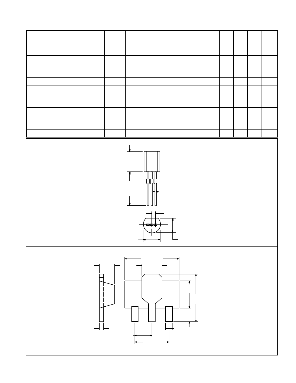
D Available in 2 Package Styles:
NTE1869 (Giant TO92 Type)
NTE1869SM (SOT–89 Surface Mount)
Applications:
D Car Stereo Equipment
D Radio Cassette Recorder
D Portable Stereo
D Other General Electronic Equipment
Absolute Maximum Ratings:
Input Voltage, V
Drive Current, I
IN
D
Input–Output Voltage Difference, V
Power Dissipation, P
D
(TA = +25°C unless otherwise specified)
I–VO
NTE1869 900mW. . . . . . . . . . . . . . . . . . . . . . . . . . . . . . . . . . . . . . . . . . . . . . . . . . . . . . . . . . . . . . . .
NTE1869SM 500mW. . . . . . . . . . . . . . . . . . . . . . . . . . . . . . . . . . . . . . . . . . . . . . . . . . . . . . . . . . . . .
Operating Temperature Range, T
Storage Temperature Range, T
opr
stg
Recommended Operating Conditions:
Supply Voltage Range, V
Rated Supply Voltage, V
IN
O
36V. . . . . . . . . . . . . . . . . . . . . . . . . . . . . . . . . . . . . . . . . . . . . . . . . . . . . . . . . . . . . . . . . .
30mA. . . . . . . . . . . . . . . . . . . . . . . . . . . . . . . . . . . . . . . . . . . . . . . . . . . . . . . . . . . . . . . . .
30V. . . . . . . . . . . . . . . . . . . . . . . . . . . . . . . . . . . . . . . . . . . . . . .
–20° to +75°C. . . . . . . . . . . . . . . . . . . . . . . . . . . . . . . . . . . . . . . . .
–55° to +150°C. . . . . . . . . . . . . . . . . . . . . . . . . . . . . . . . . . . . . . . . . .
3.5V to 30V. . . . . . . . . . . . . . . . . . . . . . . . . . . . . . . . . . . . . . . . . . . . . . . . . . .
1.5V to 25V. . . . . . . . . . . . . . . . . . . . . . . . . . . . . . . . . . . . . . . . . . . . . . . . . . . .
Electrical Characteristics: (TA = +25°C, Vi = 15V, Vo = 12V, IL = 200mA, C
unless otherwise specified)
Parameter Symbol Test Conditions Min Typ Max Unit
= 1µF, R1 = 4.3kΩ,
REF
Input Voltage V
Output Voltage V
Minimum Input–Output Voltage
VI–V
Between Pin1 and Pin2 3.5 – 36 V
IN
R2 F 0.82kΩ to 108kΩ 1.5 – 33 V
O
O
– 0.2 – V
Difference
Reference Voltage V
Input Regulation R
Load Regulation R
Bias Current I
Temperature Coefficient of Output
TC
eg–In
Between Pin3 and Pin2 1.20 1.26 1.32 V
REF
VI = 15V to 20V – 0.02 0.1 %/V
eg–LIL
B
VO
= 10mA to 200mA – 0.02 0.1 %
IL = 0 (disregarding the current in resistors
R
, R
1
2
– 1.7 3.0 mA
TA = 0° to +75°C – 0.02 – %/°C
Voltage
Ripple Rejection Ratio RR f = 120Hz – 68 – dB
Output Noise Voltage V
f = 20Hz to 100kHz – 33 – µV
NO
NTE1869
.323
(8.2)
Max
rms
.374
(9.5)
Min
.200 (5.08) Dia Max
.059
(1.5)
.024 (0.62) Max
1 2 3
.050 (1.27) Typ
.162 (4.1) Max
NTE1869SM
.174 (4.42)
.067
(1.7)
321
Pin 1. Input
2. GND
3. Reference
.096
(2.46)
.161
(4.1)
.041
(1.05)
Min
.015 (0.32)
.059 (1.5)
.118 (3.0)
Bottom View
.020 (.508)
Pin 1. Reference
2. GND
3. Input
 Loading...