

NTE1859
Integrated Circuit
dbx TV Noise Reduction Integrated Circuit
Description:
The NTE1859 is an integrated circuit designed for the dbx–TV noise reduction decode circuit for multichannel TV sound systems. This device contains a voltage controlled amplifier, a variable de–emphasis circuit with new configuration and RMS detectors with completely integrated active band pass filters, and offers the complete dbx–TV noise reduction decoder only with a few external components.
Features:
D Integrated Band Pass Filters using Active Filtering Technique and Thin Film Structure with
High Capacitance
D Variable De–emphasis Circuit with New Circuit Configuration
D Minimum Number of External Components
D Wide Operation Voltage Range: 4.7V to 16V
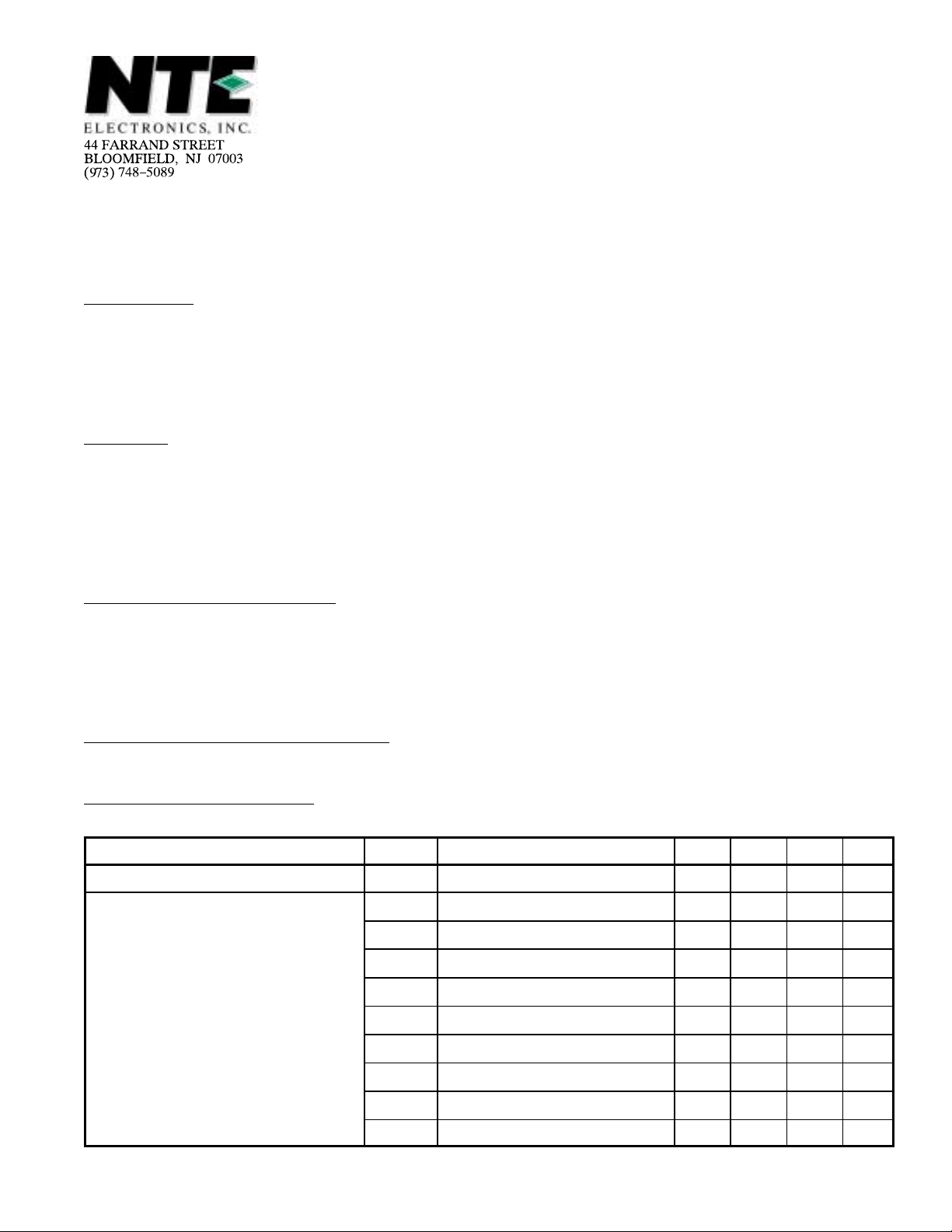
Absolute Maximum Ratings:
Power Supply Voltage, V
Allowable Power Dissipation, P
Operating Temperature Range, T
Storage Temperature Range, T
(TA = +25°C unless otherwise specified)
CC
D
opr
stg
Recommended Operating Voltage:
Power Supply Voltage, V
Electrical Characteristics:
CC
(TA = +25°C, VCC = +9V Reference Level: 0dB = –5dBm (436mVrms)
unless otherwise specified)
Parameter Symbol Test Conditions Min Typ Max Unit
Consumption Current
Decode Characteristics
I
CC
Vod–1
Vod–2
Vod–3
Vod–4
Vod–5
Vod–6
No Signal
Vi = –5dB, f = 300Hz
Vi = –15dB, f = 300Hz
Vi = –30dB, f = 300Hz
Vi = 0dB, f = 1kHz
Vi = –10dB, f = 1kHz
Vi = –20dB, f = 1kHz
17V. . . . . . . . . . . . . . . . . . . . . . . . . . . . . . . . . . . . . . . . . . . . . . . . . . . . . . . . . .
715mW. . . . . . . . . . . . . . . . . . . . . . . . . . . . . . . . . . . . . . . . . . . . . . . . .
–20° to +75°C. . . . . . . . . . . . . . . . . . . . . . . . . . . . . . . . . . . . . . . . .
–55° to +150°C. . . . . . . . . . . . . . . . . . . . . . . . . . . . . . . . . . . . . . . . . .
5V to 15V. . . . . . . . . . . . . . . . . . . . . . . . . . . . . . . . . . . . . . . . . . . . . . . . . . . . .
4.0 5.0 6.3 mA
5.5 7.0 8.5 dB
–14.5 –13.0 –11.5 dB
–44.5 –43.0 –41.5 dB
1.3 3.3 5.3 dB
–19.4 –17.4 –15.4 dB
–39.6 –37.6 –35.6 dB
Vod–7
Vod–8
Vod–9
Vi = 0dB, f = 8kHz
Vi = –10dB, f = 8kHz
Vi = –20dB, f = 8kHz
–4.3 –1.8 0.7 dB
–30.9 –28.4 –25.9 dB
–45.2 –42.7 –40.2 dB
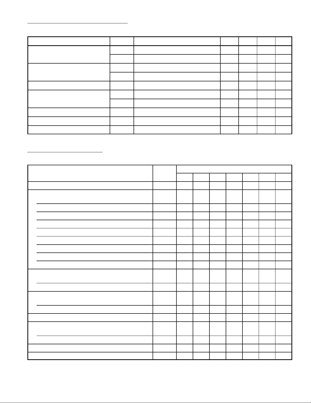
Electrical Characteristics (Cont’d): (TA = +25°C, VCC = +9V Reference Level: 0dB = –5dBm
(436mVrms) unless otherwise specified)
Parameter Symbol Test Conditions Min Typ Max Unit
VCA Filter Characteristics
Vemp. Filter Characteristics
Total Harmonic Distortion Ratio
Maximum Output Voltage
Output Noise Level
Timing Current
Center Potential
Vfp–1
Vfp–2
Vfg–1
Vfg–2
THD
Vom–1
Vom–2
V
I
time
VCC/2 4.3 4.5 4.7 V
f = 3kHz, Vi = 0dB, refer to 1kHz
f = 8kHz, Vi = 0dB, refer to 1kHz
f = 5kHz, Vi = 0dB, refer to 8kHz
f = 2kHz, Vi = 0dB, refer to 8kHz
f = 1kHz, Vi = –3dB
f = 300Hz, THD = 1.5%
f = 8kHz, THD = 1.5%
A weight
on
–5.5 –4.0 –2.5 dB
–13.0 –11.0 –9.0 dB
–9.4 –7.4 –5.4 dB
–32.3 –28.8 –25.3 dB
– 0.1 0.3 %
11.0 12.5 – dB
–2.0 1.0 – dB
– –104 –80 dB
(7.1) 7.5 (7.9) µA
Electrical Characteristics: (TA = +25°C, VCC = +9V Reference Level: 0dB = –5dBm (436mVrms)
Note 1 unless otherwise specified)
Parameter Symbol
Consumption Current I
CC
1 2 3 4 5 6 7
OFF – – – – b b
Decoding Characteristics
300Hz, –5dB
Vod–1 ON – b b b b b
300Hz, –15dB Vod–2 ON – b b b b b
300Hz, –30dB Vod–3 ON – b b b b b
1kHz, 0dB Vod–4 ON – b b b b b
1kHz, –10dB Vod–5 ON – b b b b b
1kHz, –20dB Vod–6 ON – b b b b b
8kHz, 0dB Vod–7 ON – b b b b b
8kHz, –10dB Vod–8 ON – b b b b b
8kHz, –15dB Vod–9 ON – b b b b b
VCA Filter Characteristics
3kHz
Vfp–1 ON a a b b b b
8kHz Vfp–2 ON a a b b b b
Vemp Filter Characteristics
5kHz
Vfg–1 ON b a b b b b
2kHz Vfg–2 ON b a b b b b
Total Harmonic Distortion Ratio THD ON – b b b b b
Maximum Output Voltage
300Hz
Vom–1 ON – b b b b b
8kHz Vom–2 ON – b b b b b
Output Noise Level Von OFF – b a a b b
Middle Point Potential VCC/2 OFF – – – – b b
Switch Condition
Note 1. It suffices that a or b is inserted into (–).
 Loading...