

NTE NTE1855 Datasheet

NTE1855
Integrated Circuit
Vertical Deflection Output Circuit
w
/Driver Circuit for TV Monitor
Description:
The NTE1855 is an integrated circuit in a 13–Lead SIP type package that contains the vertical deflection output circuit with a driver for small–aperture (maximum deflection current 1.8A
TV, monitor/display use. This device has such features as greatly reduced number of external parts
and low power dissipation. Since both DC feedback and AC feedback can be provided inside the IC,
it is easy to design the vertical deflection circuit.
Features:
D Low Power Dissipation due to On–Chip Pump–Up Circuit
D On–Chip 50/60Hz Vertical Size Control Circuit
D On–Chip Driver Circuit
D Vertical Output Circuit
D On–Chip Thermal Protection Circuit
D Minimum Number of External Parts Required
) color/B & W
p–p
Absolute Maximum Ratings
Driver Power Supply Voltage, +V
Pump–Up Power Supply Voltage, +V
Output Power Supply Voltage, +V
Deflection Output Current, I
: (TA = +25°C unless otherwise specified)
1max 15V. . . . . . . . . . . . . . . . . . . . . . . . . . . . . . . . . . . . . . . . . . . . . .
CC
7max 30V. . . . . . . . . . . . . . . . . . . . . . . . . . . . . . . . . . . . . . . . . .
CC
12max 62V. . . . . . . . . . . . . . . . . . . . . . . . . . . . . . . . . . . . . . . . . . . .
CC
–1.5 to +1.5A
. . . . . . . . . . . . . . . . . . . . . . . . . . . . . . . . . . . . . . . . . .
DEF
Allowable Power Dissipation (With Infinite Heat Sink), P
Operating Temperature Range, T
Storage Temperature Range, T
Thermal Resistance, Junction–to–Case, R
Operating Supply Voltage Conditions:
Driver Supply Voltage, +V
CC
Pump–Up Supply Voltage, +V
Recommended Operating Conditions:
Driver Supply Voltage, +V
CC
Pump–Up Supply Voltage +V
Deflection Output Current, I
opr
stg
tnJC
(TA = +25°C unless otherwise specified)
1 8V to 14V. . . . . . . . . . . . . . . . . . . . . . . . . . . . . . . . . . . . . . . . . . . . . . . . . . .
7 10V to 27V. . . . . . . . . . . . . . . . . . . . . . . . . . . . . . . . . . . . . . . . . . . . .
CC
(TA = +25°C unless otherwise specified)
1 12V. . . . . . . . . . . . . . . . . . . . . . . . . . . . . . . . . . . . . . . . . . . . . . . . . . . . . . . .
7 24V. . . . . . . . . . . . . . . . . . . . . . . . . . . . . . . . . . . . . . . . . . . . . . . . . . . . .
CC
11p–p
. . . . . . . . . . . . . . . . . . . . . . . . . . . . . . . . . . . . . . . . . . . .
max 8W. . . . . . . . . . . . . . . . . . . . . . . . . . . .
D
–20° to +85°C. . . . . . . . . . . . . . . . . . . . . . . . . . . . . . . . . . . . . . . . .
–40° to +150°C. . . . . . . . . . . . . . . . . . . . . . . . . . . . . . . . . . . . . . . . . .
up to 1.8A
P–O
4°C/W. . . . . . . . . . . . . . . . . . . . . . . . . . . . . . . . . . . . . . .
P–P
Electrical Characteristics: (TA = +25°C, +VCC1 = 12V, +VCC7 = 24V unless otherwise specified)
Parameter Symbol Test Conditions Min Typ Max Unit
Driver Power Supply Quiescent Current I
Trigger Input Threshold Voltage V
Vertical Size Control Pin Voltage V
Ramp Waveform Shape Start Voltage V
Pump–Up Charge Saturation Voltage V
Pump–Up Discharge Saturation Voltage V
Deflection Output Saturation Voltage, Lower V
Deflection Output Saturation Voltage, Upper V
Idling Current 8 18 32 mA
Voltage Gain G
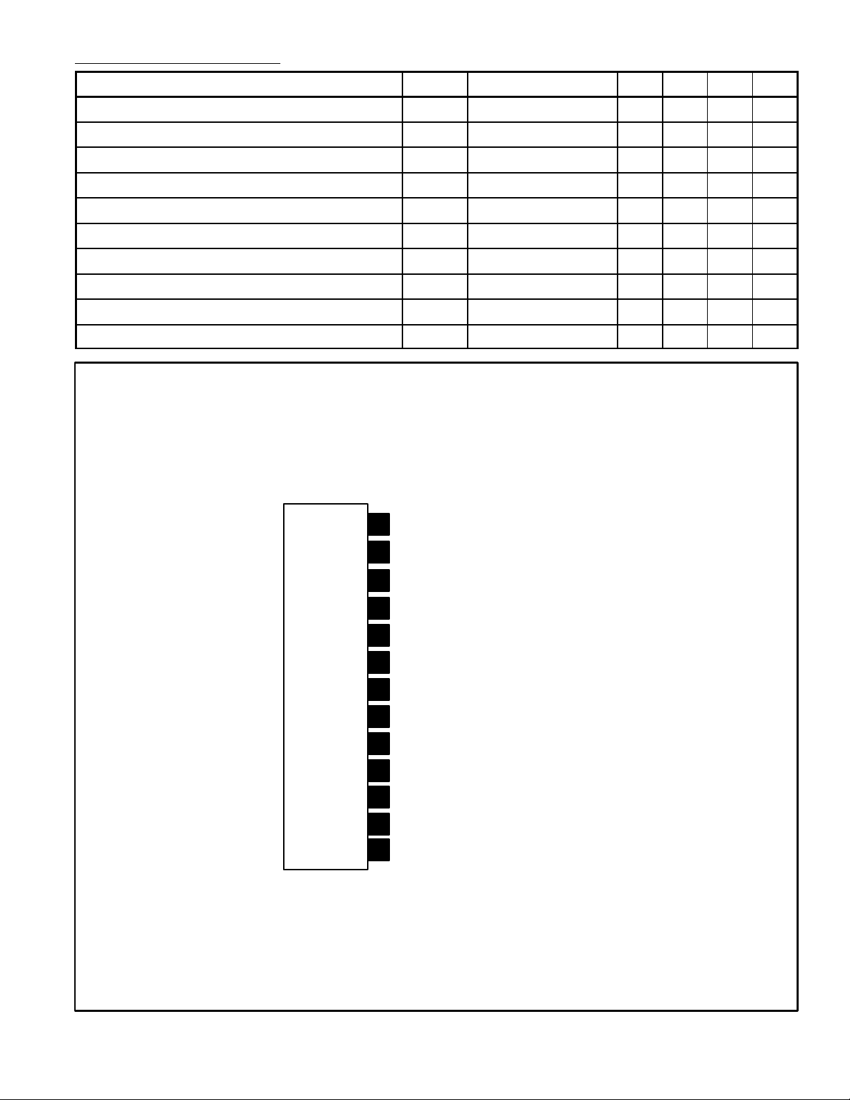
Pin Connection Diagram
CC1
2
3
Ramp
S8–10
S7–8
S11–10
S12–11
VO
(Front View)
I = 900mA – – 3.0 V
I = 900mA – – 1.2 V
I = 900mA – – 3.2 V
f = 1kHz – 59 – dB
1.8 2.8 3.8 mA
2.8 3.1 3.4 V
5.9 6.1 6.3 V
4.7 5.0 5.3 V
– – 1.5 V
Ripple Filter
13
12
Power Supply for Vertical Output
11
Vertical Output
GND
10
9
OSC Blocking
8
Pump–Up Output
7
VCC7
6
AC/DC Feedback Input to Vertical Output Section
5
Ramp Waveform Generator
4
50/60Hz Vertical Size Control Signal Input
Vertical Height Control
3
V ertical Trigger Input
2
1
V
CC
1
 Loading...