


NTE1854D/NTE1854M
Integrated Circuit
Dual Power Operational Amplifier
Description:
The NTE1854D/NTE1854M is a monolithic dual–power operational amplifier which features a high
current, low saturation voltage, flyback protected output stage optimized for driving heavy inductive
loads. Capable of operation in a single supply mode form as low as 4.5V up to 13.2V, the
NTE1854D/NTE1854M is ideally suited for the computer peripheral environment, driving small motors, solenoids, and linear actuators in an H–bridge configuration.
As a general–purpose op amp, the NTE1854D/NTE1854M exhibits low input offset voltage, high open
loop gain, low quiescent current, a large differential input voltage range, and a common–mode input
voltage range which includes ground (V
Features:
D Full output swing at ±500mA
D High inductive load drive capability
D Internal flyback protection diodes
D Low power dissipation
D Single or split supply operation
D Common–mode range includes ground (VEE)
D High open loop gain
D Low input offset voltage
D Large differential input voltage range
D Thermal shutdown protection
D Available in Two Package Types:
NTE1854M: 8–Lead Mini DIP
NTE1854D: 14–Lead DIP
EE
).
Absolute Maximum Ratings:
Supply Voltage (Single Supply), V
DC Output Current, I
OUT
Peak Output Current (Non–Repetitive), I
Common–Mode Input Voltage, V
Differential–Mode Input Voltage, V
Operational Junction Temperature, T
Storage Temperature Range, T
Lead Temperature (During Soldering, 10sec), T
(Note 1)
CC
ICM
IDM
J
stg
–0.3V to 14V. . . . . . . . . . . . . . . . . . . . . . . . . . . . . . . . . . . . . . . . . .
OUT
–0.3V to VCC –2V. . . . . . . . . . . . . . . . . . . . . . . . . . . . . . . . . . . . . .
. . . . . . . . . . . . . . . . . . . . . . . . . . . . . . . . . . . . . . . . . . . . . . . .
+150°C. . . . . . . . . . . . . . . . . . . . . . . . . . . . . . . . . . . . . . . . . . . . . .
–65°C to 150°C. . . . . . . . . . . . . . . . . . . . . . . . . . . . . . . . . . . . . . . . .
L
+300°C. . . . . . . . . . . . . . . . . . . . . . . . . . . . . . . . . . . .
±1.0A. . . . . . . . . . . . . . . . . . . . . . . . . . . . . . . . . . . . . . . . . . . . . . . . . . . . . . . . . .
±1.5A. . . . . . . . . . . . . . . . . . . . . . . . . . . . . . . . . . . . . . . . .
±V
CC
Note 1 Exceeding these ratings could cause damage to the device. All voltages are with respect
to GND. All currents are positive into the specified terminal.
Recommended Operating Conditions:
Supply Voltage (Single Supply), V
DC Output Current, I
OUT
Common–mode Input Voltage, V
Differential–Mode Input Voltage, V
CC
ICM
IDM
. . . . . . . . . . . . . . . . . . . . . . . . . . . . . . . . . . . . . . . . . . . . . . . .
Operating Ambient Temperature Range, T
4.5V to 13.2V. . . . . . . . . . . . . . . . . . . . . . . . . . . . . . . . . . . . . . . . .
±500mA. . . . . . . . . . . . . . . . . . . . . . . . . . . . . . . . . . . . . . . . . . . . . . . . . . . . . . . .
0V to VCC –2V. . . . . . . . . . . . . . . . . . . . . . . . . . . . . . . . . . . . . . . .
±V
CC
A
0°C to 70°C. . . . . . . . . . . . . . . . . . . . . . . . . . . . . . . . . . . . .
Electrical Specifications:
(VCC = 12V, TA = 25°C, unless otherwise specified.)
Parameter Symbol Test Conditions Min Typ Max Unit
STATIC CHARACTERISTICS
Input Offset Voltage V
Input Bias Current I
Input Offset Current I
OS
Difference Input Resistance R
Source Side Output Saturation Voltage (+) V
Sink Side Output Saturation Voltage (–)V
Open Loop Voltage Gain A
VOL
IO
TA = T
B
TA = T
ID
SATIOUT
I
OUT
SATIOUT
I
OUT
to T
MIN
MIN
to T
MAX
MAX
= –100mA – 0.8 – V
= –500mA – 1.0 1.5 V
= –100mA – 0.3 – V
= –500mA – 0.6 1.0 V
–15 0 +15 mV
–30 – +30 mV
–1.0 –0.2 – µA
–50 – +50 nA
–200 – +200 nA
500 – – KΩ
70 90 – dB
Common–Mode Rejection Ratio CMRR 66 90 – dB
Power Supply Rejection Ratio PSRR 60 80 – dB
Quiescent Drain Current I
CC
– 7 15 mA
Thermal Shutdown Temperature – 175 – °C
DYNAMIC CHARACTERISTICS
Gain Bandwidth Product GBWP RL = ∞Ω – 800 – kHz
Slew Rate dVO/dt AV = 1 – 1.6 – V/µs
Power Bandwidth, –3dB PBW – 200 – kHz
Input Noise Voltage E
Input Noise Current I
Channel Separation C
22Hz to 22kHz – 10 – µV
N
22Hz to 22kHz – 200 – pA
N
f = 1kHz, RL = 10Ω,
S
AV
= 30dB
CL
– 60 – dB
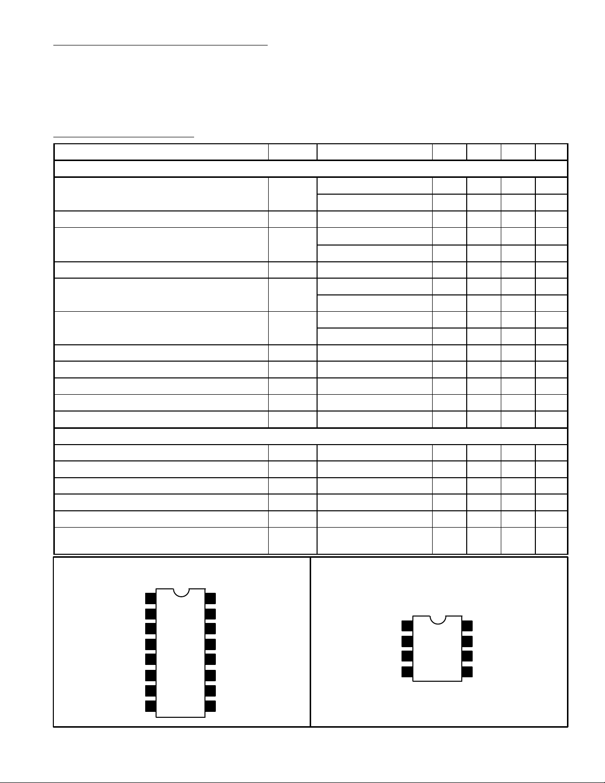
Pin Connection Diagram
Supply Voltage
Output 2
GND
NTE1854D
1
2
3
4
5Inverted Input 2
6Non–Inverted Input 2
7Non–Inverted Input 1
8Inverted Input 1 9 GND
GNDOutput 1
16
15
GND
14
GND
13
GND
12 GND
11 GND
10 GND
Pin Connection Diagram
Output 1
Supply Voltage
Output 2
GND
NTE1854M
1
2
3
4
Inverted Input 1
8
Non–Inverted Input 1
7
Non–Inverted Input 2
6
Inverted Input 2
5
 Loading...