

NTE1853
Integrated Circuit
Digital Filter for Compact Disc Digital Audio System
Features:
D 16–Bit Serial Data Input (Two’s Complement)
D Interpolated Data Replaces Erroneous Data Samples
D –12dB Attenuation via the Active Low Attenuation Input Control (ATSB)
D Smoothed Trasitions Before and After Muting
D Two Identical Finite Impulse Response Transversal Filters each with a Sampling Rate of Four
Times that of the Normal Digital Audio Data
D Digital Audio Output of 32–Bit Words Transmitted in Biphasemark Code
Applications:
D Compact Disc Digital Audio System
D Digital Filter
Absolute Maximum Ratings:
Supply Voltage Range (Pin24), V
Maximum Input Voltage Range, V
Electrostatic Handling (Note 2), V
DD
I
ES
Operating Ambient Temperature Range, T
Storage Temperature Range, T
stg
A
–0.5V to +7.0V. . . . . . . . . . . . . . . . . . . . . . . . . . . . . . . . . . . . . . . .
–0.5V to VDD+0.5V. . . . . . . . . . . . . . . . . . . . . . . . . . . . . . . . . . . . . .
–1000V to +1000V. . . . . . . . . . . . . . . . . . . . . . . . . . . . . . . . . . . . .
–20° to +70°C. . . . . . . . . . . . . . . . . . . . . . . . . . . . . . . . . . .
–65° to +150°C. . . . . . . . . . . . . . . . . . . . . . . . . . . . . . . . . . . . . . . . . .
Note 1. All outputs are short–circuit protected except the crystal oscillator output.
Note 2. Equivalent to discharging a 100pF capacitor through a 1.5Ω series resistor with a rise time
of 15ns.
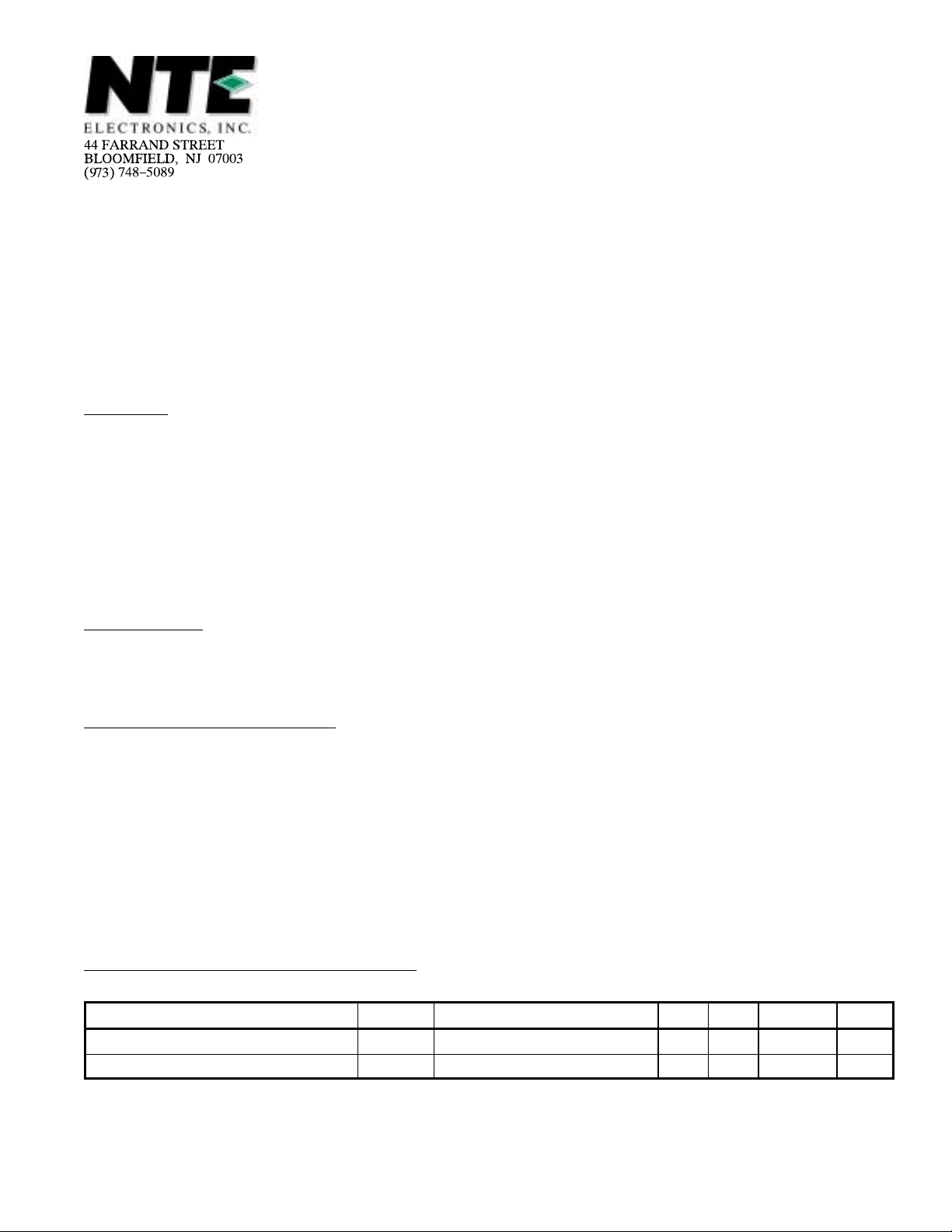
DC and AC Electrical Characteristics:
(VDD = 4.5 to 5.5V, VSS = 0, TA = –20° to +70°C unless
otherwise specified)
Parameter Symbol Test Conditions Min Typ Max Unit
Supply Voltage (Pin24) V
Supply Current (Pin24) I
DD
DD
4.5 5.0 5.5 V
– 180 – mA
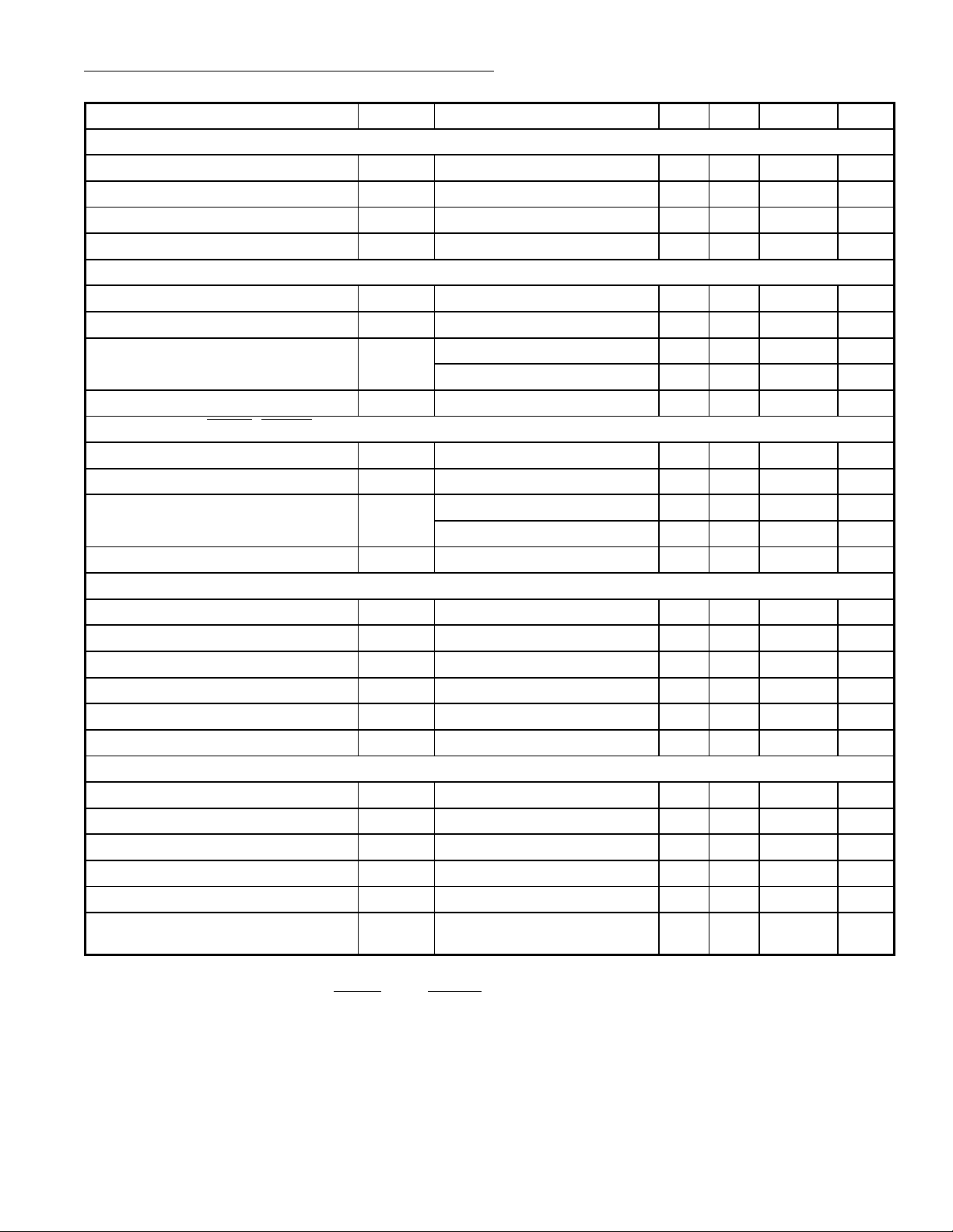
DC and AC Electrical Characteristics (Cont’d): (VDD = 4.5 to 5.5V, VSS = 0, TA = –20° to +70°C
unless otherwise specified)
Parameter Symbol Test Conditions Min Typ Max Unit
WSAB, DAAB
Input Voltage, Low V
Input Voltage, High V
Input Leakage Current I
Input Capacitance C
EFAB, SDAB (Note 1)
Input Voltage, Low V
Input Voltage, High V
Input Leakage Current I
Input Capacitance C
CLAB, SCAB, ATSB, MUSB (Note 2)
Input Voltage, Low V
Input Voltage, High V
Input Leakage Current I
Input Capacitance C
Output XOUT
Mutual Conductance at 100kHz G
Small–Signal Voltage Gain A
Input Capacitance C
Feedback Capacitance C
Output Capacitance C
Input Leakage Current I
Slave Clock Mode
Input Voltage (Peak to Peak) V
I(P–P)
Input Voltage, Low V
Input Voltage, High V
Input Rise Time t
Input Fall Time t
Input High Time at 2V (Relative to
t
HIGH
Clock Period)
IH
LI
IH
LI
IH
LI
FB
LI
IH
R
F
IL
I
IL
VI = 0V –10 – – µA
VI = V
DD
I
IL
VI = 0V –30 – – µA
VI = V
DD
I
M
AV = GM x R
V
I
O
O
Note 3 3.0 – VDD+0.5 V
Note 3 0 – 1 V
IL
Note 3 3.0 – VDD+0.5 V
Note 4 – – 20 ns
Note 4 – – 20 ns
–0.3 – +0.8 V
2.0 – VDD+0.5 V
–10 – +10 µA
– – 7 pF
–0.3 – +0.8 V
2.0 – VDD+0.5 V
– – +50 µA
– – 7 pF
–0.3 – +0.8 V
2.0 – VDD+0.5 V
– – +10 µA
– – 7 pF
1.5 – – mA/V
3.5 – – V/V
– – 10 pF
– – 5 pF
– – 10 pF
–10 0 +10 µA
35 – 65 %
Note 1. Inputs EFAB and SDAB both have internal pull–downs.
Note 2. Inputs CLAB, SCAB, ATSB
, and MUSB have internal pull–ups.
Note 3. The minimum peak–to–peak voltage can be reduced to 2V if the output XSYS is not being
used. Similarly V
can be reduced to 2.4V (Min). All other levels remain the same.
IH
Note 4. Reference levels = 10% and 90%.
 Loading...