

NTE NTE1850 Datasheet

NTE1850
Integrated Circuit
Dual 12W/Channel Audio Power Amplifier
Description:
The NTE1850 is a dual Hi–Fi audio power amplifier in a 9–Lead SIP type package designed for
mains–fed applications such as stereo TV sound and stereo radio. The circuit is optimal for symmetrical power supplies but is also well suited to asymmetrical power supply systems. An output power
of 2 x 12W (THD = 0.5%) can be delivered into an 8Ω load with a symmetrical power supply of ±16V.
The gain is fixed internally at 30dB, but can be changed externally if required. Internal gain fixing gives
low gain spread and very good balance between the amplifiers (0.2dB).
A special feature is an input mute circuit which provides suppression of unwanted signals at the inputs
during switching on and off. This circuit disconnects the non–inverting inputs when the supply voltage
is below ±6V, while allowing the amplifiers to remain in their DC operating condition.
Two thermal p rotection c ircuits a re p rovided, o ne m onitors t he a verage j unction t emperature a nd t he o ther
the instantaneous t emperature o f t he p ower transistors. B oth p rotection c ircuits activate a t + 150°C, a llowing safe operation to a maximum junction temperature of +150°C without added distortion.
Features:
D Few External Components Required
D Input Muted During Power ON/OFF
D Low Offset Voltage Between Output and GND
D Excellent Gain Balance Between Channels
D Short–Circuit Protected
D Thermally Protected
Applications:
D Stereo
D TV Sound
D Radio
Absolute Maximum Ratings:
Supply Voltage (Pin5 and Pin7), VCC = V5,
7–3
Non–Repetitive Peak Output Current (Pin4 and Pin6), I
Total Power Dissipation (T
= +25°C, Infinite Heatsink), P
A
Derate Above 25°C 2.5°C/W. . . . . . . . . . . . . . . . . . . . . . . . . . . . . . . . . . . . . . . . . . . . . . . . . . . . . . .
Operating Junction Temperature, T
Storage Temperature Range, T
J
stg
Short–Circuit Time (Outputs Short–Circuited to GND), t
Thermal Resistance, Junction–to–Case, R
thJC
OSM
TOT
SC
+20V. . . . . . . . . . . . . . . . . . . . . . . . . . . . . . . . . . . . . . . .
4A. . . . . . . . . . . . . . . . . . . . . . . . . . . . . . .
15W. . . . . . . . . . . . . . . . . . . . . . . . . . .
+150°C. . . . . . . . . . . . . . . . . . . . . . . . . . . . . . . . . . . . . . . . . . . . . . .
–65° to +150°C. . . . . . . . . . . . . . . . . . . . . . . . . . . . . . . . . . . . . . . . . .
1Hr. . . . . . . . . . . . . . . . . . . . . . . . . . . . . . .
25°C/W. . . . . . . . . . . . . . . . . . . . . . . . . . . . . . . . . . . . .
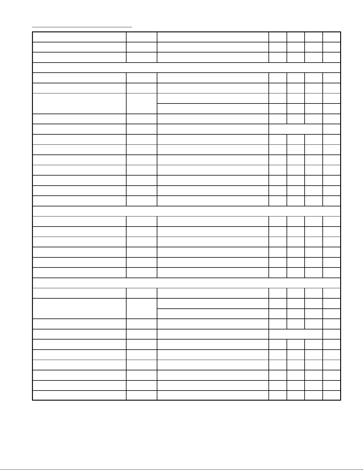
DC Electrical Characteristics:
Parameter Symbol Test Conditions Min Typ Max Unit
Supply Voltage Range V
Repetitive Peak Output Current I
CC
ORM
– ±16 ±20 V
– – 2.2 A
Operating Mode (Symmetrical Power Supply, VCC = ±16V, RL = 8Ω, TA = +25°C, f = 1kHz)
Supply Voltage Range V
Total Quiescent Current I
Output Power P
CC
TOT
O
Without R
L
THD = 0.5% 10 12 – W
±7.5 ±16 ±20 V
– 50 – mA
THD = 10% 10 15 – W
Total Harmonic Distortion THD PO = 6W – – 0.2 %
Power Bandwidth B THD = 0.5%, Note 1 20Hz to 20kHz
Voltage Gain G
Noise Output Voltage V
NO(RMS)RS
V
= 2kΩ, unweighted (20Hz to 2okHz) – 70 140 µV
29 30 31 dB
Input Impedance |Zi| 14 20 26 kΩ
Ripple Rejection RR Note 2 40 60 – dB
Channel Separation ∞ RS = 0Ω 46 70 – dB
Input Bias Current I
DC Output Offset Voltage V
IB
OFF
WRT GND – 20 200 mV
– 0.3 – µA
Input Mute Mode (Symmetrical Power Supply, VCC = ±4V, RL = 8Ω, TA = +25°C, f = 1kHz)
Supply Voltage V
Total Quiescent Current I
Output Voltage V
Noise Output Voltage V
NO(RMS)RS
CC
TOT
OUT
Without R
L
VI = 600mV – – 1.8 mV
= 2kΩ, unweighted (20Hz to 2okHz) – 70 140 µV
±2 – ±5.8 V
– 30 – mA
Ripple Rejection RR Note 2 35 – – dB
DC Output Offset Voltage V
OFF
WRT GND – 20 200 mV
Operating Mode (Asymmetrical Power Supply, VCC = ±4V, RL = 8Ω, TA = +25°C, f = 1kHz)
Total Quiescent Current I
Output Power P
TOT
Without R
THD = 0.5% 5 6 – W
O
L
– 50 – mA
THD = 10% 5 8.5 – W
Total Harmonic Distortion THD PO = 4W – – 0.2 %
Power Bandwidth B THD = 0.5%, Note 1 40Hz to 20kHz
Voltage Gain G
Gain Balance ∆G
Noise Output Voltage V
NO(RMS)RS
V
V
= 2kΩ, unweighted (20Hz to 2okHz) – 70 140 µV
29 30 31 dB
– 0.2 – dB
Input Impedance |Zi| 14 20 26 kΩ
Ripple Rejection RR Note 2 40 50 – dB
Channel Separation ∞ RS = 0Ω 40 – – dB
Note 1. Power Bandwidth at P
O(MAX)
= –3dB.
Note 2. Ripple Rejection at RS = 0Ω, f = 100Hz to 20kHz; ripple voltage = 200mV (RMS value) applied
to positive or negative supply rail.
 Loading...