

NTE NTE1849 Datasheet
NTE1849
Integrated Circuit
Frequency Synthesizer for TV Tuning Systems
Description:
The NTE1849 is a CMOS frequency synthesizer for TV tuning systems consisting of a 13–bit programmable divider, 12–bit divider and phase comparator circuits.
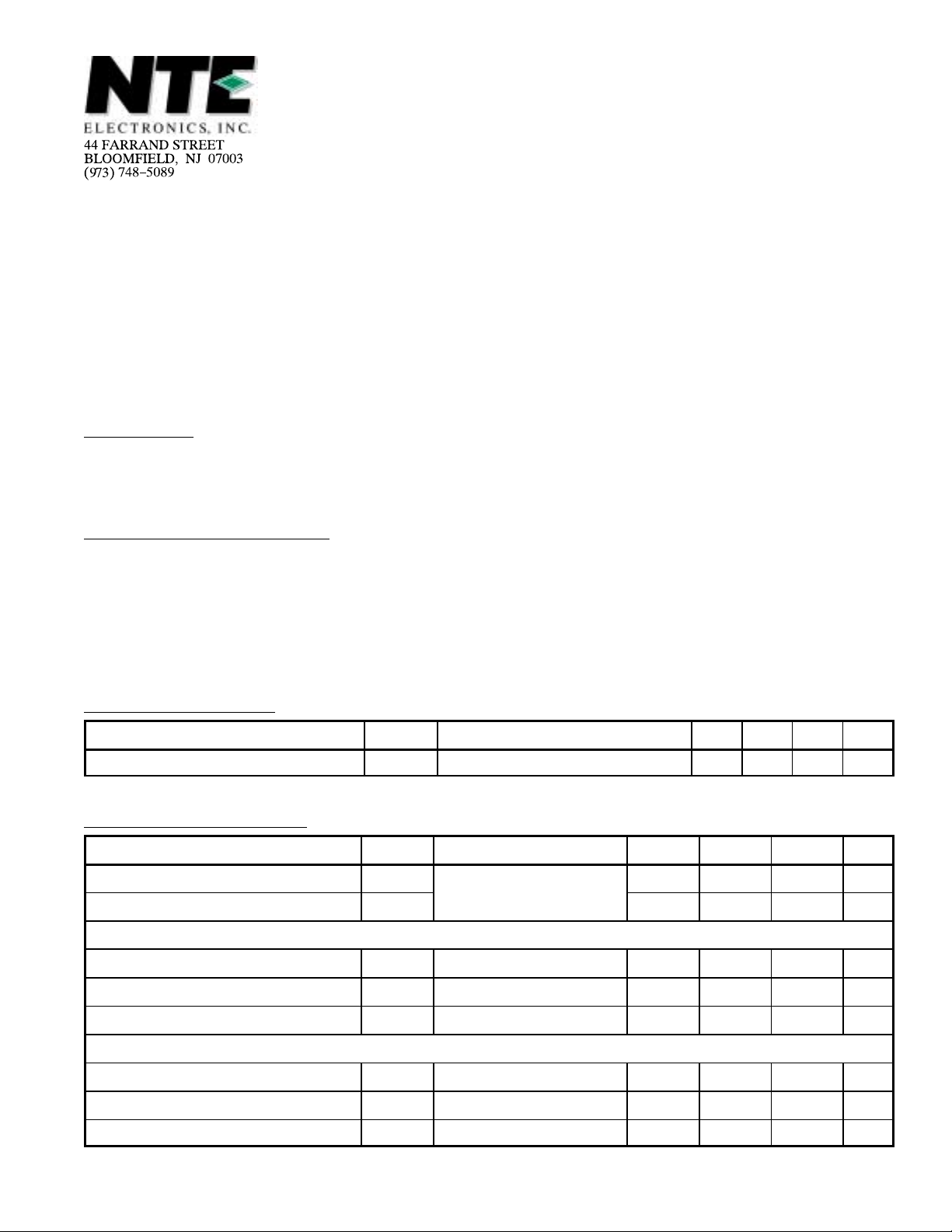
Absolute Maximum Ratings
Supply Voltage, V
Input Voltage, V
Output Voltage, V
DD
I
O
Operating Temperature Range, T
Storage Temperature Range, T
Operating Conditions
: (VSS = 0V, TA = 0° to +70°C unless otherwise specified)
: (VSS = 0V, TA = +25°C unless otherwise specified)
–0.3 to VDD +0.3V. . . . . . . . . . . . . . . . . . . . . . . . . . . . . . . . . . . . . . . . . . . . . . . . . . . . . .
–0.3 to VDD +0.3V. . . . . . . . . . . . . . . . . . . . . . . . . . . . . . . . . . . . . . . . . . . . . . . . . . . .
opr
stg
–0.3 to +9V. . . . . . . . . . . . . . . . . . . . . . . . . . . . . . . . . . . . . . . . . . . . . . . . . . . . . . . . .
–20° to +70°C. . . . . . . . . . . . . . . . . . . . . . . . . . . . . . . . . . . . . . . . .
–55° to +100°C. . . . . . . . . . . . . . . . . . . . . . . . . . . . . . . . . . . . . . . . . .
Parameter Symbol Test Conditions Min Typ Max Unit
Supply Voltage V
DD
6.5 7.0 7.5 V
Electrical Characteristics: (VDD = 7V, VSS = 0V, TA = 0° to +70°C unless otherwise specified)
Parameter Symbol Test Conditions Min Typ Max Unit
Supply Current I
Total Power Dissipation P
Input Terminal (LFI)
Maximum Input Signal Frequency f
i(max)
Input Voltage Swing V
Input Current I
Input Terminal (PI0 to PI3, LDI)
DD
tot
I(1)
TA = +25°C, VDD = 7V,
TA = +25 C, VDD = 7V,
without load
Input Sine Wave, 15.6 – – MHz
Free Running LFI 0.7 – – V
i
VI = VSS to V
DD
– – 15 mA
– – 105 mW
–50 – +50 µA
p–p
“H” Level Input Voltage V
“L” Level Input Voltage V
Input Current I
IH
IL
I(2)
VI = VSS to V
DD
3.4 – V
V
SS
– 0.8 V
DD
V
–10 – +10 µA
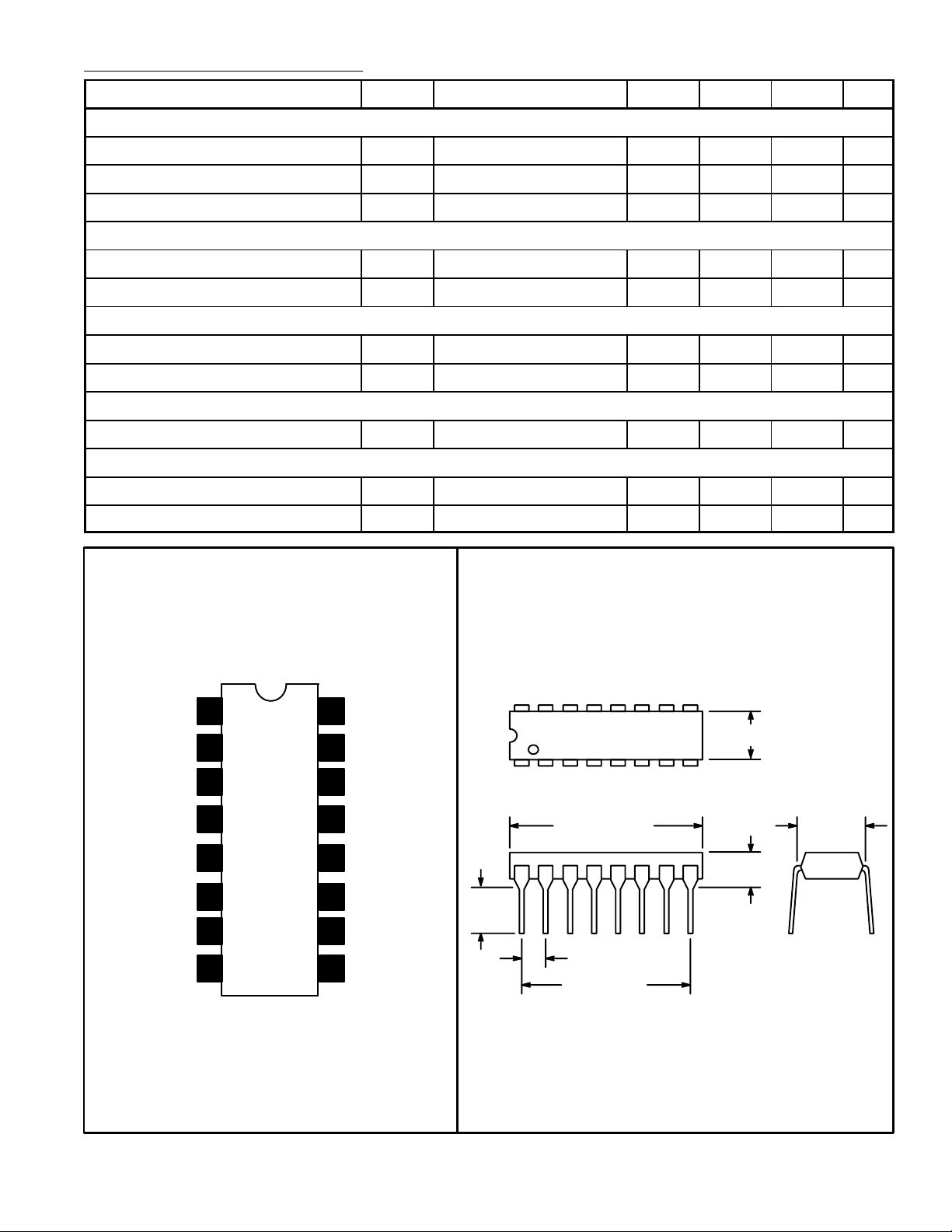
Electrical Characteristics (Cont’d): (VDD = 7V, VSS = 0V, TA = 0° to +70°C unless otherwise specified)
Parameter Symbol Test Conditions Min Typ Max Unit
Output Terminal (PDO)
“H” Level Output Current I
“L” Level Output Current I
Output Leakage Current I
OH(1)
OL(1)
Leak
OutputTerminal (TMO)
“H” Level Output Voltage V
“L” Level Output Voltage V
OH(1)IOH
OL(1)IOL
Output Terminal (CKO)
“H” Level Output Voltage V
“L” Level Output Voltage V
OH(2)IOH
OL(2)IOL
Oscillator Terminal (QI, QO)
Oscillation Frequency f
OSC
Capacitance
Input Capacitance C
Output Capacitance C
VO = 5V –0.8 – – mA
VO = 2V 0.8 – – mA
VO = 1/2 V
DD
–0.03 – +0.03 µA
= –0.05mA 6.0 – – V
= 0.1mA – – 0.4 V
= –0.4mA 6.0 – – V
= 0.16mA – – 0.4 V
– 3.58 – MHz
VI = 2V – 5 – pF
I
VO = 2V – 7 – pF
O
Pin Connection Diagram
V
QO
CKO PI2
LDI
TMO
N.C.
PDO
DD
QI
1
2
3
4
5
6
7
8
16
15
14
13
12
11
10
9
V
SS
LFI
PI3
PI1
PI0
SCO
RCO
.245
(6.22)
Min
16 9
.260 (6.6) Max
18
.785 (19.9)
Max
.200 (5.08)
Max
.100 (2.54)
.700 (17.7)
.300
(7.62)
 Loading...