

NTE NTE1843 Datasheet
NTE1843
Integrated Circuit
FM Front End
Description:
The NTE1843 is an integrated circuit in a 9–Lead SIP type package designed for use in FM front–end
applications. Typical applications include portable radio and radio cassettes.
Compared with conventional types, supply voltage dependence, overload characteristics and spurious radiation characteristics are improved.
Features:
D Wide Supply Voltage Range: VCC = 1.6V to 6.0V
D Excellent Supply Voltage Dependence of Loacl Oscillator: Oscillator Stop V
D Improved Inter–Modulation Charactristics by Double Balanced Type Mixer Circuit
D Low Spurious Radiation
D Built–In Clamping Diode for the Local Oscillator Output
= 0.9V Typ
CC
Absolute Maximum Ratings:
Supply Voltage, V
Power Dissipation, P
CC
D
(TA = +25°C unless otherwise specified)
Derate Above 25°C 4mW/°C. . . . . . . . . . . . . . . . . . . . . . . . . . . . . . . . . . . . . . . . . . . . . . . . . . . . . . .
Operating Temperature Range, T
Storage Temperature Range, T
Electrical Characteristics:
(TA = +25°C, VCC = 5V, f = 83MHz, fm = 1kHz, ∆f = 22.5kHz dev. unless
opr
stg
otherwise specified)
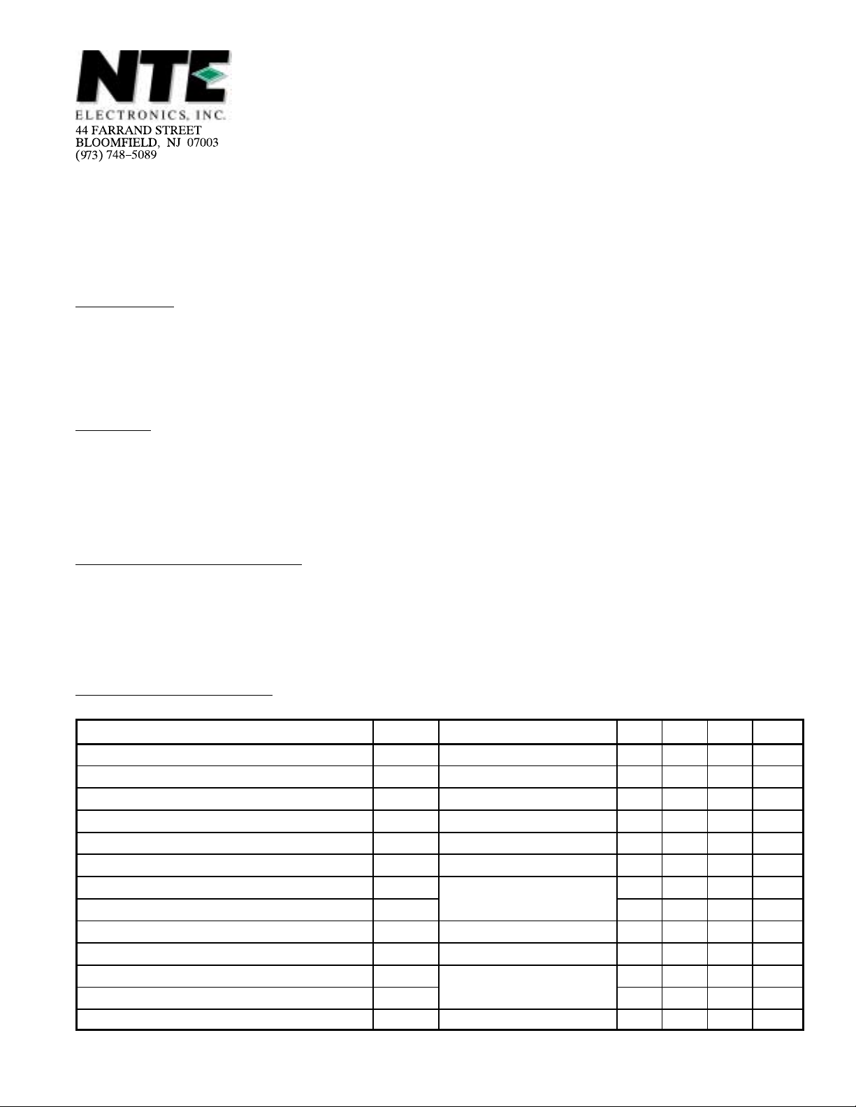
Parameter Symbol Test Conditions Min Typ Max Unit
Supply Current I
–3dB Limiting Sensitivity V
Quiescent Sensitivity Q
Conversion Gain G
Local OSC Voltage V
Parallel Input Resistance (Pin1 Impedance) r
Parallel Output Resistance (Pin3 Impedance) r
Parallel Output Capacitance (Pin3 Impedance) c
Parallel Input Resistance (Pin4 Impedance) r
Parallel Input Capacitance (Pin4 Impedance) c
Parallel Output Resistance (Pin6 Impedance) r
Parallel Output Capacitance (Pin6 Impedance) c
Local OSC Stop Voltage V
CC
in(lim)
OSCfOSC
ip1
op3
op3
ip4
ip4
op6
op6
stop
VIN = 0 – 5.2 8.0 mA
S
C
f = 83MHz – 25 – kΩ
f = 10.7MHz – 100 0 kΩ
500mW. . . . . . . . . . . . . . . . . . . . . . . . . . . . . . . . . . . . . . . . . . . . . . . . . . . . . . . . . .
–25° to +75°C. . . . . . . . . . . . . . . . . . . . . . . . . . . . . . . . . . . . . . . . .
–55° to +150°C. . . . . . . . . . . . . . . . . . . . . . . . . . . . . . . . . . . . . . . . . .
– 3.0 7.0 dBµ
– 11 – dBµ
– 31 – dB
= 60MHz 150 230 350 mV
– 57 – Ω
– 2.0 – pF
– 2.7 – kΩ
– 3.3 – pF
– 4.8 – pF
– 0.9 1.3 V
8V. . . . . . . . . . . . . . . . . . . . . . . . . . . . . . . . . . . . . . . . . . . . . . . . . . . . . . . . . . . . . . . . .
rms
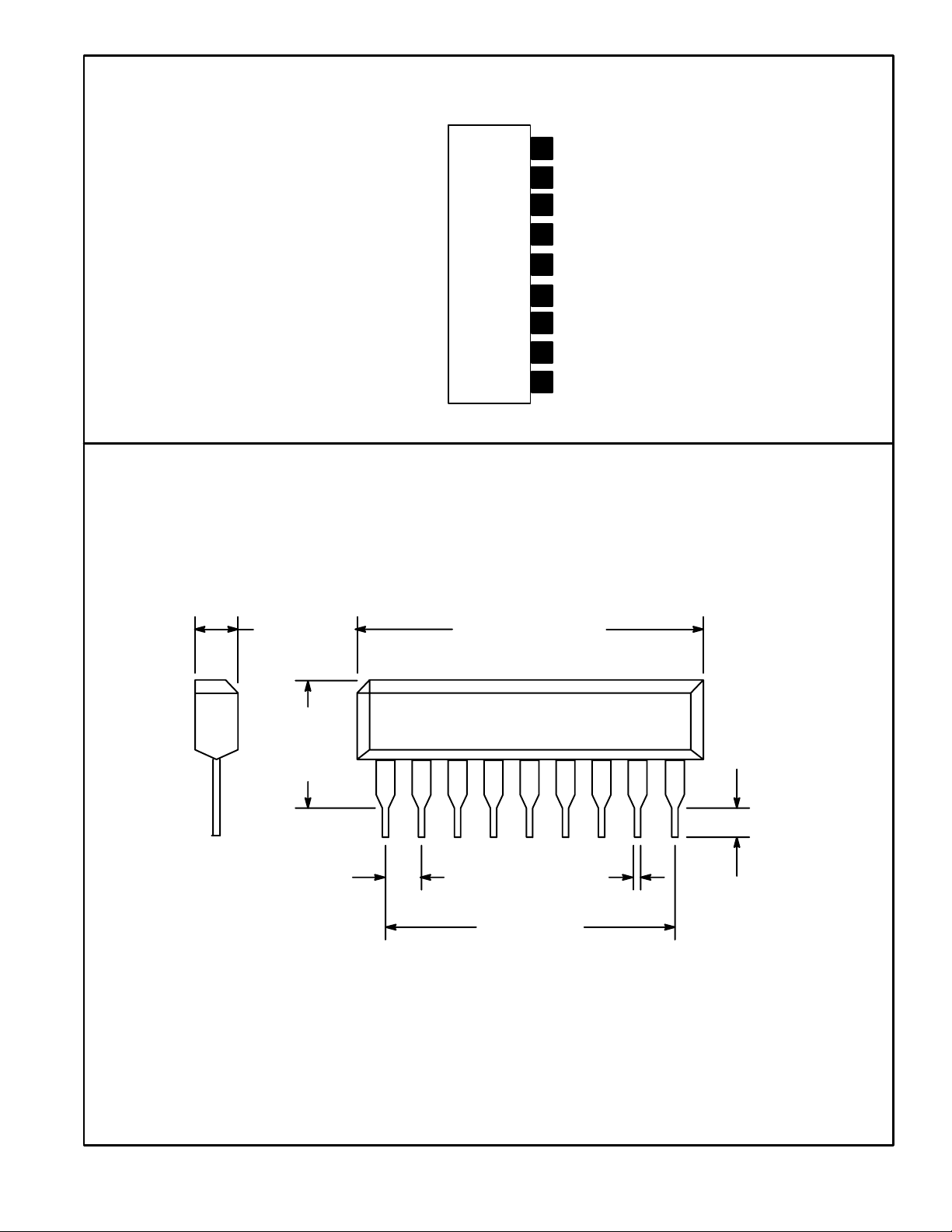
Pin Connection Diagram
(Front View)
9
V
OSC Output
8
OSC Input
7
6
Mixer Output
GND
5
4
Mixer Input
3
Tuning Coil
2
Bypass
RF Input
1
CC
.323
(8.2)
Max
.100 (2.54)
.906 (23.0) Max.126 (3.2)
19
.020 (0.50)
.099
(2.5)
.800 (20.3)
Min
 Loading...