

NTE NTE1830, NTE1831 Datasheet
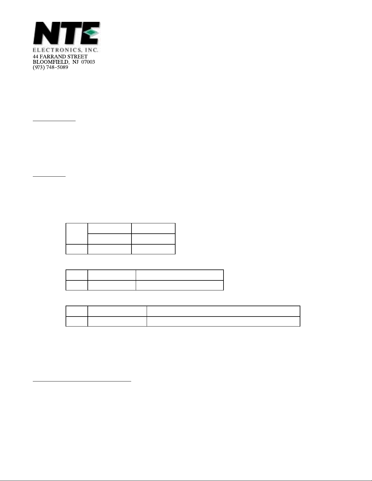
NTE1830 & NTE1831
Integrated Circuit
Dual Audio Power Amplifier, 5.8W (19W BTL)
Description:
The NTE1830 and NTE1830 are dual audio power amplifiers in a 12–Lead DIP type package for use
in consumer applications. Designed for high power, low distortion, and low noise, these devices contain various types of protection circuitry making them suitable for high performance car audio power
amplifier applications.
Features:
D Two Kinds of Pin Configurations:
Normal (NTE1830)
Reverse (NTE1831)
D Operating Supply Voltage Range: VCC(opr) = 9V to 18V
D High Power: (V
BTL
Dual 5.8W (Typ) THD = 10%
= 13.2V, f = 1kHz, RL = 4Ω)
CC
19W (Typ) THD = 10%
15W (Typ) THD = 1%
D Low Distortion: (VCC = 13.2V, f = 1kHz, RL = 4Ω)
BTL
0.03% (Typ) P
Dual 0.06% (Typ) P
= 4W, GV = 40dB
OUT
= 1W, GV = 52dB
OUT
D Low Noise: (VCC = 13.2V, RL = 4Ω)
BTL
0.14mV
Dual 0.7mV
(Typ) GV = 40dB, Rg = 0, DIN NOISE: DIN 45405
rms
(Typ) GV = 52dB, Rg = 10kΩ, BW = 20Hz to 20kHz
rms
D Protector:
Thermal Shut–Down
Overvoltage Protection
BTL–OCL DC Short Protection
Absolute Maximum Ratings:
Peak Supply Voltage (0.2sec), V
DC Supply Voltage, V
DC 25V. . . . . . . . . . . . . . . . . . . . . . . . . . . . . . . . . . . . . . . . . . . . . . . . . . . . . . . . . .
CC
Operating Supply Voltage, V
Peak Output Current, I
Power Dissipation, P
peak 4.5A. . . . . . . . . . . . . . . . . . . . . . . . . . . . . . . . . . . . . . . . . . . . . . . . . . . . . . .
O
D
Operating Temperature Range, T
Storage Temperature Range, T
(TA = +25°C unless otherwise specified)
surge 45V. . . . . . . . . . . . . . . . . . . . . . . . . . . . . . . . . . . . . . . . . . . . . .
CC
opr 18V. . . . . . . . . . . . . . . . . . . . . . . . . . . . . . . . . . . . . . . . . . . . . . . . . . . .
CC
opr
stg
25W. . . . . . . . . . . . . . . . . . . . . . . . . . . . . . . . . . . . . . . . . . . . . . . . . . . . . . . . . . . . .
–30° to +75°C. . . . . . . . . . . . . . . . . . . . . . . . . . . . . . . . . . . . . . . . .
–55° to +150°C. . . . . . . . . . . . . . . . . . . . . . . . . . . . . . . . . . . . . . . . . .
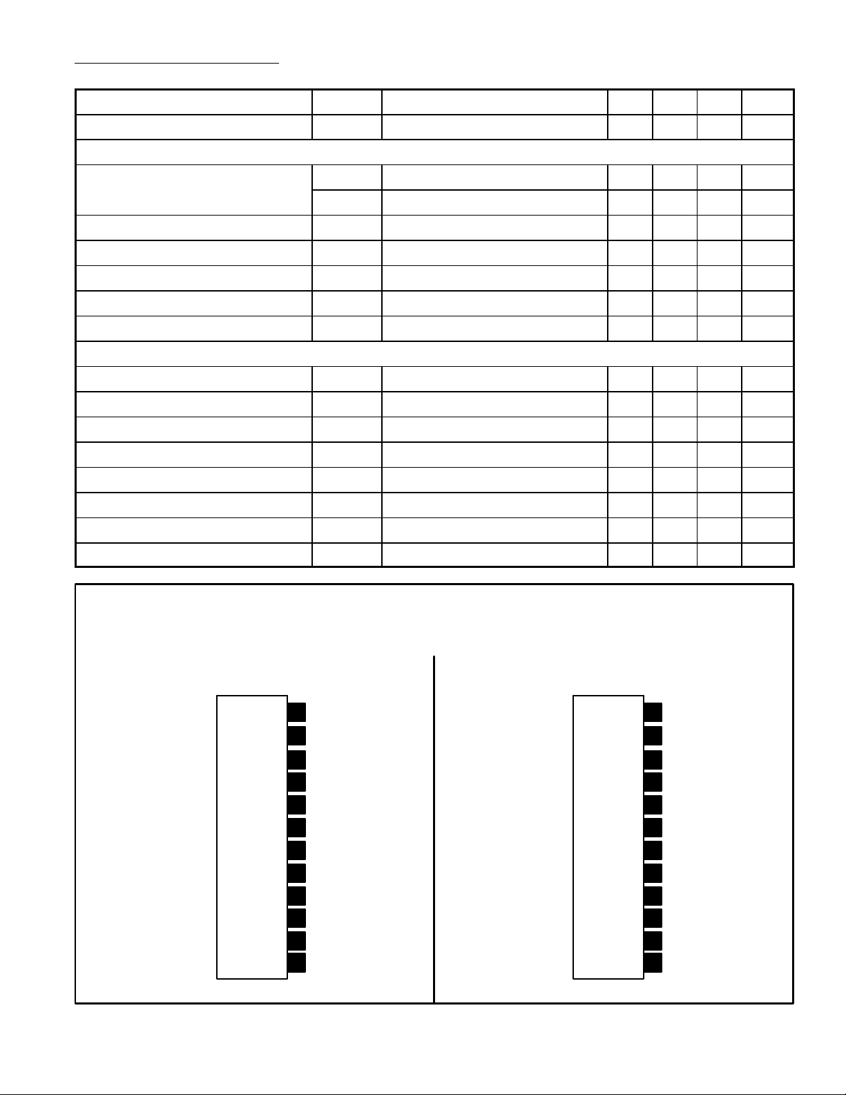
Electrical Characteristics: (TA = +25°C, VCC = 13.2V, RL = 4Ω, Rg = 600Ω, f = 1kHz unless
otherwise specified)
Parameter Symbol Test Conditions Min Typ Max Unit
Quiescent Current I
CCQ
VIN = 0 – 80 145 mA
BTL Connection Mode
Output Power P
Total Harmonic Distortion THD (1) P
Output Offset Voltage V
Voltage Gain GV (1) V
(1) THD = 10% 16 19 – W
OUT
P
(2) THD = 1% 12 15 – W
OUT
= 4W, GV = 40dB – 0.03 0.25 %
OUT
OFF
VIN = 0 – 0 0.35 V
= 0dBm – 40 – dB
OUT
Output Noise Voltage VNO (1) Rg = 0, DIN 45405 Noise Filter – 0.14 – mV
Ripple Rejection Ratio RR (1) f
= 100Hz, V
ripple
= 0dBm – –52 –40 dB
ripple
Dual Mode
Output Power P
Total Harmonic Distortion THD (2) P
Voltage Gain GV (2) V
Voltage Gain Ratio ∆G
(3) THD = 10% 5.0 5.8 – W
OUT
= 1W – 0.06 0.30 %
OUT
= 0dBm 50 52 54 dB
OUT
V
V
= 0dBm –1 0 +1 dB
OUT
Output Noise Voltage VNO (2) Rg = 10kΩ, BW = 20Hz to 20kHz – 0.7 1.5 mV
Ripple Rejection Ratio RR (2) f
Crosstalk CT V
Input Resistance R
IN
= 100Hz, V
ripple
= 0dBm – –57 – dB
OUT
= 0dBm – –52 –40 dB
ripple
f = 1kHz – 33 – kΩ
rms
rms
Pin Connection Diagram
NTE1830 NTE1831
Output 2
12
Bootstrap 2
11
V
10
CC
Bootstrap 1
9
Output 1
8
PWR–GND
7
(+) Input 1
6
(–) NF 1
5
Pre–GND
4
Ripple Filter
3
(–) NF 2
2
(+) Input 2
1
(Front View)
(+) Input 2
12
(–) NF 2
11
Ripple Filter
10
Pre–GND
9
(–) NF 1
8
(+) Input 1
7
PWR–GND
6
Output 1
5
Bootstrap 1
4
3
V
CC
Bootstrap 2
2
Output 2
1
 Loading...