

NTE NTE1818 Datasheet
NTE1818
Integrated Circuit
Module, AF PO, 25W/Ch,
Dual Power Supply
Features:
D Muting circuit to cut off pop noise
D Greatly reduced heat sink due to case temperature +125°C guaranteed
Absolute Maximum Ratings: (TA = +25°C unless otherwise specified)
Maximum Supply Voltage, V
CC max
Thermal Resistance, Junction–to–Case, R
Junction Temperature, T
150°C. . . . . . . . . . . . . . . . . . . . . . . . . . . . . . . . . . . . . . . . . . . . . . . . . . . . . . . . .
J
Operating Case Temperature, T
Storage Temperature Range, T
Available Time for Load Shorted (V
±39V. . . . . . . . . . . . . . . . . . . . . . . . . . . . . . . . . . . . . . . . . . . . . . . . . .
thJC
125°C. . . . . . . . . . . . . . . . . . . . . . . . . . . . . . . . . . . . . . . . . . . . . . . . . .
C
–30° to +125°C. . . . . . . . . . . . . . . . . . . . . . . . . . . . . . . . . . . . . . . . . .
stg
= ±26V, RL = 8Ω, f = 50Hz, PO = 25W), t
CC
2.6°C/W. . . . . . . . . . . . . . . . . . . . . . . . . . . . . . . . . . . . .
s
2sec. . . . . . . . . . .
Recommended Operating Conditions
Recommended Operating Voltage, V
Load Resistance, R
Operating Characteristics
Parameter Symbol Test Conditions Min Typ Max Unit
Quiescent Current I
Output Power
Total Harmonic Distortion THD PO = 1.0W, f = 1kHz – – 0.3 %
Frequency Response fL, f
Input Resistance ri PO = 1.0W, f = 1kHz – 55 – kΩ
Output Noise Voltage V
Midpoint Voltage V
Muting Voltage V
8Ω. . . . . . . . . . . . . . . . . . . . . . . . . . . . . . . . . . . . . . . . . . . . . . . . . . . . . . . . . . . . . . . .
L
: (TA = +25°C, VCC = ±26V, RL = 8Ω, Rg = 600Ω, VG = 40dB,
R
: non–inductive load, unless otherwise specified)
L
: (TA = +25°C unless otherwise specified)
±26V. . . . . . . . . . . . . . . . . . . . . . . . . . . . . . . . . . . . . . . . . . . . . .
CC
CCO
P
P
O(1)
O(2)
NO
VCC = ±31V 20 40 100 mA
THD – 0.4%, f = 20Hz ∼ 20kHz 25 – – W
VCC = ±22V, THD = 1.0% 25 – – W
PO = 1.0W, –3dB 20 to 50k Hz
H
VCC = ±31V. Rg = 10kΩ – – 1.2 mV
VCC = ±31V –70 0 70 mV
N
M
–2 –5 –10 V
rms
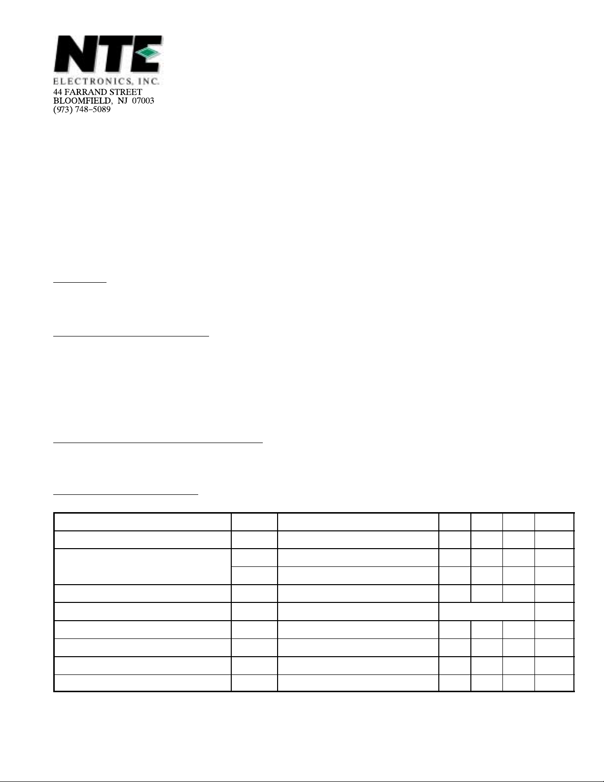
Pin Connection Diagram
18 Rt Ch Input (–)
17
Rt Ch Input (+)
16
GND
15
Compensation
14
(–) V
CC
13
Rt Ch Output
Bypass
12
11
(+) V
CC
10
Lt Ch Output
9
(–) V
CC
8
Compensation
7
Compensation
6 Muting
Compensation
5
4
Compensation
3
Compensation
2
Lt Ch Input (+)
Lt Ch Input (–)
1
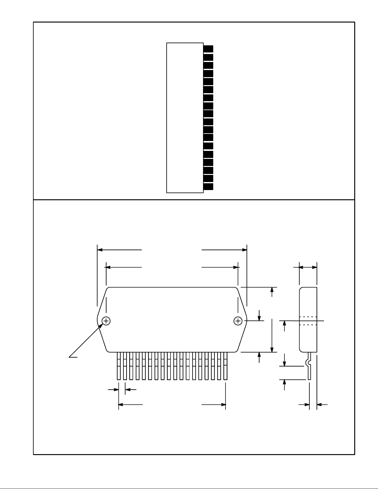
.141
(3.6)
Dia
(2 Holes)
2.520 (64.0)
2.190 (55.6)
.334 (8.5)
1.440
(36.4)
.737
118
(18.7)
1.030
(32.5)
.158 (4.0)
.100 (2.54)
1.700 (43.18)
.114 (5.5)
 Loading...