

NTE NTE1814 Datasheet
NTE1814
Integrated Circuit
CMOS, Color Processing Circuit for VCR
Description:
The NTE1814 is a CMOS LSI integrated circuit in an 18–Lead DIP type package designed for use
in VCR color signal processing circuits for VHS system video tape recorders. This device is used in
configuration with the NTE1813 for color signal processing in 2, 4, and 6Hr modes in NTSC VCR systems.
Features:
D In Recording, a Video Color Signal can be Converted into a Low–Frequency Video Color Signal
by AFC and REC APC.
D In Playback, the Low–Frequency Color Signal can be Converted into the Original Video Color
Signal on the Color Subcarrier Wave Frequency by PB APC and the Side Lock Detect Circuit.
D The NTE1814 Contains the Following Functions:
Rotary Circuit
DPLL (Digital Phase Locked Loop) Circuit
Side Lock Detect Circuit
Field Start Inhibit Pulse Generating Circuit
Burst Adjust Pulse Generating Circuit
Burst Gate Pulse Generating Circuit
Monostable Multivibrator Circuit
Phase Comparator
D Can be Miniaturized and Simplified with High Reliability
D Low Power Dissipation: 15mW @ 5V
Absolute Maximum Ratings:
Supply Voltage, V
Input Voltage, V
Output Votage, V
DD
I
O
Operating Ambient Temperature Range, T
Storage Temperature Range, T
(TA = +25°C unless otherwise specified)
opr
stg
–0.3 to +8.0V. . . . . . . . . . . . . . . . . . . . . . . . . . . . . . . . . . . . . . . . . . . . . . . . . . . . . . .
–0.3V to VDD+0.3V. . . . . . . . . . . . . . . . . . . . . . . . . . . . . . . . . . . . . . . . . . . . . . . . . . . . .
–0.3V to VDD+0.3V. . . . . . . . . . . . . . . . . . . . . . . . . . . . . . . . . . . . . . . . . . . . . . . . . . . .
–10° to +70°C. . . . . . . . . . . . . . . . . . . . . . . . . . . . . . . . . .
–55° to + 125°C. . . . . . . . . . . . . . . . . . . . . . . . . . . . . . . . . . . . . . . . .
Recommended Operating Conditions: (VSS = 0V, TA = +25°C ±2°C unless otherwise specified)
Parameter Symbol Test Conditions Min Typ Max Unit
Supply Voltage V
VCO Input Operating Frequency f
VCO Input Amplitude V
DD
VCO
VCO
NTSC – 5.03 – MHz
C cut (C = 1000pF) Sine Wave Input 0.3 0.5 – V
4.5 5.0 5.5 V
P–P
DC Electrical Characteristics: (VDD = 5V, VSS = 0V, TA = +25°C ±2°C, f
unless otherwise specified)
Parameter Symbol Test Conditions Min Typ Max Unit
= 5.03MHz (NTSC)
VCO
Supply Current I
Power Dissipation P
Input Terminal 1
PGI, SYN
Input Terminal 2
SCM, PN, NREC, BERR, TPB
(with a Pull–Low Resistance)
(with a Pull–Low Resistance)
Input Terminal 3
NCLR
(with a Pull–High Resistance)
(with a Pull–High Resistance)
Output Terminal 1
HP, PSSC
Output Terminal 2
LOC, PCO, BADJ, BGP
(3–Value Output)
(3–Value Output)
Output Terminal 3 FSI I
V
V
V
I
I
I
I
I
Leak2VO
I
DD
IH1
V
IH2
V
I
IH2
IH3
V
I
IH3
OH1
OL1
OH2
OL2
OH3
OL3
No Load – – 3 mA
No Load – – 15 mW
tot
3.5 – V
IL1
IL2
VI = 5V – – 300 µA
IL3
VI = 0V – – –300 µA
VOH = 3.5V –0.5 – – mA
VOL = 1.5V 0.5 – – mA
VOH = 2.5V –2.5 –5.0 – mA
VOL = 2.5V 2.5 5.0 – mA
= 5V, 0V (with a High Impedance) – – ±5 µA
VOH = 4.3V –0.5 – – mA
VOL = 0.7V 0.5 – – mA
V
3.5 – V
V
3.5 – V
V
– 1.5 V
SS
– 1.5 V
SS
– 1.5 V
SS
DD
DD
DD
V
V
V
V
DD
VCO Clock Input
NTSC/PAL/SECAM
Select Input (SCM)
Horiz Pulse Output
NTSC/PAL/SECAM
Select Input (PN)
Head Switch Pulse Input
Side Lock Detect Output
V
SS
Phase Comparator Output
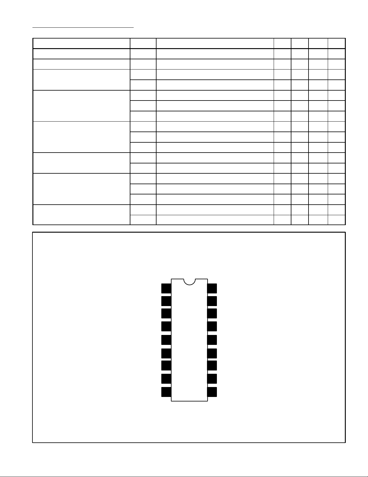
Pin Connection Diagram
1
2
3
4
5
6
7
8
18
17
16
15
14
13
12
11
9 10
Burst Gate Pulse Output
Special PB Select Input
Low Converting Color
Subcarrier Wave Output
System Clear Input
Sync Signal Input
Field Start Inhibit Pulse Output
Burst Compensation
Error Pulse Input
Rec/PB Select Input
Burst Compensation Pulse Output
 Loading...