

NTE NTE1813 Datasheet
NTE1813
Integrated Circuit
Color Signal Processor for VCR
Description:
The NTE1813 is an integrated circuit in a 22–Lead DIP type package. When combined with the
NTE1814, this device provides the functions which process VCR color signals at the 2H/4H/6H mode
is NTSC systems.
Features:
D Low Operating Supply Voltage: VCC = 5V
D Low Power Consumption: 110mW
D AFC and APC System in Recording Mode. APC System Only During Playback Mode.
D Better S/N Ratio by Chroma ACC (2H/6H Mode).
Absolute Maximum Ratings:
Supply Voltage, V
Power Dissipation (T
CC
= +70°C), P
A
(TA = +25°C unless otherwise specified)
D
Operating Ambient Temperature Range, T
Storage Temperature Range, T
Electrical Characteristics:
Parameter Symbol Test Conditions Min Typ Max Unit
Total Circuit Current I
REC Output Amplitude (Burst ACC) v
REC ACC Control Sensitivity (Burst ACC) b
Chroma ACC b
Main BM Amp Gain G
Main BM carrier Leak CL
Burst Emphasis Amount G
REC Current Up Rate G
PB Output Amplitude (2H) v
Burst De–Emphasis Amount G
stg
(TA = +25°C, VCC = 5V unless otherwise specified)
O14–R
AGC–B
AGC–C
O14–P
opr
tot
V–16
16
E11
REC
DE
250mW. . . . . . . . . . . . . . . . . . . . . . . . . . . . . . . . . . . . . . . . . . . . . .
–20° to +70°C. . . . . . . . . . . . . . . . . . . . . . . . . . . . . . . . . .
–40° to +150°C. . . . . . . . . . . . . . . . . . . . . . . . . . . . . . . . . . . . . . . . . .
15 – 32 mA
Pin22 Input Burst 0.1V
+6dB to –15dB – – 3 dB
Pin20 Input 0.5V
Pin20 Input 0.25V
Pin20 Input 0.25V
Pin1 Input 0.2V
Pin1 Input 0.2V
P–P
P–P
P–P
P–P
P–P
P–P
0.5 – 1.2 V
0.5 – 4.5 dB
4 – 9 dB
– – –33 dB
5 – 7 dB
0.5 – 2.5 dB
0.2 – 0.55 V
–6.5 – –4.5 dB
P–P
P–P
6V. . . . . . . . . . . . . . . . . . . . . . . . . . . . . . . . . . . . . . . . . . . . . . . . . . . . . . . . . . . . . . . . .
Note 1. Operating Supply Voltage: V
CC(opr)
= 4.5V to 5.5V.
Electrical Characteristics (Cont’d): (TA = +25°C, VCC = 5V unless otherwise specified)
Parameter Symbol Test Conditions Min Typ Max Unit
PB/REC Crosstalk CT
REC Control Voltage S
Sub BM Amp Gain G
Sub BM Carrier leak CL
Killer Sensitivity (ON) K
Killer Sensitivity (OFF) K
Killer Output (LOW) V
VCO FREE Frequency f
VCO Control Sensitivity b
VCO Output Amplitude v
REC Pull–In Range (H) f
REC Pull–In Range (L) f
2H Mode Range S
4H Mode S
6H Mode S
Note 1. Operating Supply Voltage: V
CC(opr)
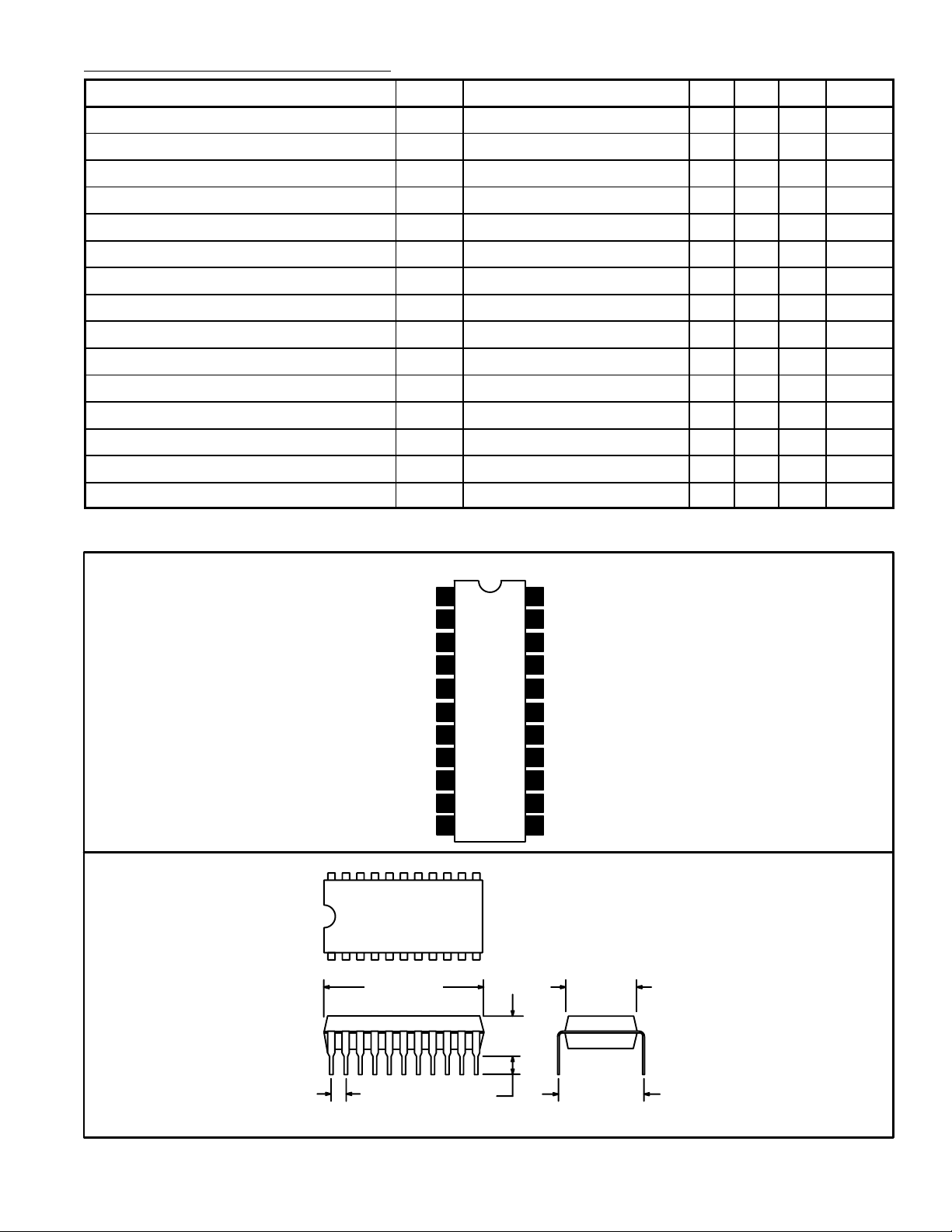
Pin Connection Diagram
PB Chroma Input/
Rec Changeover Input
ACC Burst Detector
ACC Reference
X’tal OSC Input
Burst Gate Pulse Input
Sub BM Output
V
Sub BM Input
2/4/6H Select
VCO Output
14–P
1–REC
Pin9 Input 0.65V
V–7
7
gate1
gate2
14–L
OSC
O11
APC–H
APC–L
10–1
10–2
10–3
Pin20 Input 0dB = 0.25V
Pin20 Input 0dB = 0.25V
2
= 4.5V to 5.5V.
1
2
3
4
5X’tal OSC Output
6
7
8
CC
9 14
10 13
11 12
P–P
3.58MHz Chroma
22
Input
21
ACC Output
ACC Input
20
19
Killer Control
18
Main BM Input
17
GND
16
PB Main BM Output
X’tal APC Control
15
Chroma Output
VCO Control
VCO Adjust
P–P
P–P
– – –40 dB
4.6 – – V
1 – 5 dB
– – –35 dB
–22 – – dB
– – –10 dB
– – 0.5 V
3 – 7 MHz
1.5 – 3.5 kHz/mV
0.4 – – V
P–P
500 – – Hz
– – –500 Hz
– – 0.6 V
1.6 – 2.0 V
3.2 – 3.6 V
22 12
111
.756 (19.2) .252 (6.4)
.177
(4.5)
.070 (1.78)
.135 (3.43)
.300 (7.62)
 Loading...