

NTE NTE1801 Datasheet

NTE1801
Integrated Circuit
TV dbx Noise Reduction System
Description:
The NTE1801 Multiplexed Sound dbx Noise Reduction Decoder is a single–chip linear IC in a
28–Lead DIP type package suitable for US NTSC System use. The device incorporates two RMS–
level sensors and VCA circuits, as well as five operational amplifiers and two buffer circuits.
A complete multiplexed sound system for US NTSC System television sets can be built by interfacing
the NTE1801 with the NTE1800 Multiplexed Sound Decoder.
Features:
D Low Distortion Ratio, Low Interference
D Low Power Supply Current
D Single, 8V to 15V Power Supply
D 100mV
D Easily Interfaced to the NTE1800
Functions:
D On–Chip dbx Noise Reduction Decoder and VCA Circuits
D On–Chip RMS Level Sensor
D L + R Signal Buffer Amplifier
(300Hz, 0dB) Input Voltage (Pin4)
rms
Absolute Maximum Ratings: (TA = +25°C unless otherwise specified)
Supply Voltage, VCCmax 15V. . . . . . . . . . . . . . . . . . . . . . . . . . . . . . . . . . . . . . . . . . . . . . . . . . . . . . . . . . . .
Power Dissipation (TA = +75°C), PD 580mW. . . . . . . . . . . . . . . . . . . . . . . . . . . . . . . . . . . . . . . . . . . . . . .
Operating Temperature Range, T
Storage Temperature Range, T
stg
opr
–20° to +75°C. . . . . . . . . . . . . . . . . . . . . . . . . . . . . . . . . . . . . . . . .
–40° to +125°C. . . . . . . . . . . . . . . . . . . . . . . . . . . . . . . . . . . . . . . . . .
Recommended Operating Conditions: (TA = +25°C unless otherwise specified)
Parameter Symbol Test Conditions Min Typ Max Unit
Power Supply Voltage
Input Signal Voltage
Amp 1 Gain
Amp 2 Gain
V
CC
V
AV1 0 10.3 30.0 dB
AV2 0 – 20 dB
f = 300Hz, Pin4
IN
8.0 12.0 13.5 V
– 100 – mV
rms
Operating Characteristics: (TA = +2 5°C, VCC = 12V, 0dB = 100mV
Parameter Symbol Test Conditions Notes Min Typ Max Unit
unless otherwise specified)
rms
Circuit Current I
Output Voltage V
V
V
V
V
V
V
Maximum Output Voltage V
Total Harmonic Distortion
Output Noise Voltage NL1 Rg = 0, 400 to 30kHz using BPF (L–R) – –96 –90 dBV
Reference Voltage V
THD1 VO = 0dB, f = 1kH z,
THD2 VO = 215mV, f = 1kHz,
NL2 (L+R) – –90 –70 dBV
No Signal – 8.0 12.5 17.0 mA
CC
f = 300Hz, VIN = +10dB (L–R) +17 +20 +23 dB
O1
f = 300Hz, VIN = 0dB (L–R) –3 0 +3 dB
O2
f = 300Hz, VIN = –20dB (L–R) –43 –40 –37 dB
O3
f = 8kHz, VIN = +17dB (L–R) +12.1 +15.1 +18.1 dB
O4
f = 8kHz, VIN = +7 dB (L–R) –14.6 –11.6 –8.6 dB
O5
f = 8kHz, VIN = –3dB (L–R) –43.6 –40.6 –37.6 dB
O6
f = 1kHz, VIN = 215mV (L+R) –0.5 0 +0.5 dB
O7
f = 1kHz, THD = 1%,
OM
(400 to 300kHz using BPF)
(400 to 300kHz using BPF)
(400 to 300kHz using BPF)
VCC = 12V – 5.8 6.0 6.2 V
ref
(L–R) 4.0 8.6 – V
(L–R) – 0.1 0.5 %
(L+R) – 0.1 0.3 %
Caution: Static Electricity can impair the performance of this device.
P–P
GND
Non–Invert Input (Amp 1)
Invert Input (Amp 1)
Preamp Output
Buffer Input
Capacitor
RMS Detector 2 Input
Capacitor
Resistor Adjust
Non–Invert Input (Amp 5)
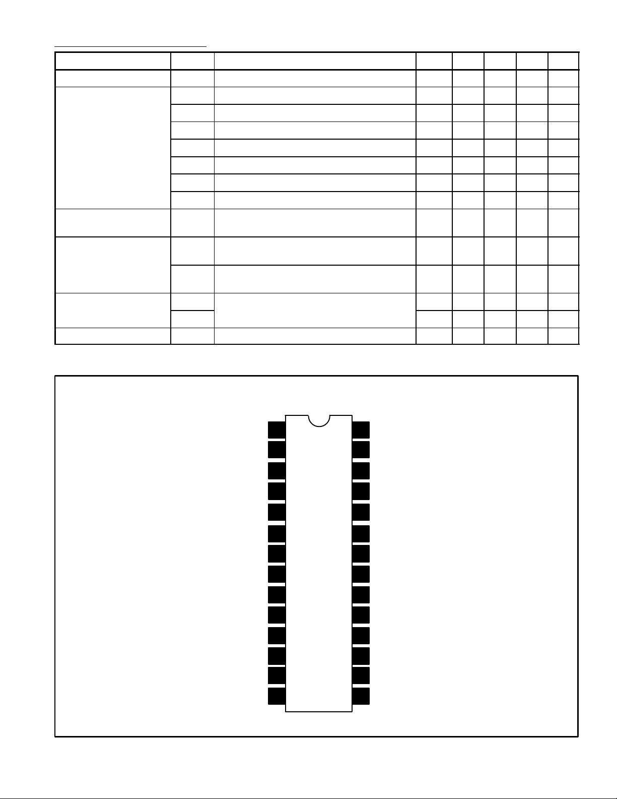
Pin Connection Diagram
1
2
3
4
5
6Buffer Output
7RMS Detector 1 Input
8
9
10
11
28
27
26
25
24
23
22
21
20
19
18
13Invert Input (Amp 5) 16
Reference Voltage
Capacitor
Buffer Input
Buffer Output
VCA1 Input
VCA1 Adjust
N.C.
N.C.
Input (Amp 3)
Output (Amp 3)
VCA2 Input
Input (Amp 4)12 17
L–R/SAP Output
V
14 15
CC
L+R Output
 Loading...