

NTE1797
Integrated Circuit
Color TV Vertical Output Circuit
Description:
The NTE1797 is a monolithic linear IC designed for large–aperture color TV vertical deflection output
and has such features as greatly reduced number of external parts and low power dissipation. The
NTE1797 can be used in conjunction with the NTE1845 for video chroma deflection use and the
NTE1538 for deflection use.
Features:
D High Output
D On–Chip Pump–Up Circuit and Low Power Dissipation
D Minimum Number of External Parts Required
Absolute Maximum Ratings: (TA = +25°C unless otherwise specified)
Maximum Supply Voltage, V8max 30V. . . . . . . . . . . . . . . . . . . . . . . . . . . . . . . . . . . . . . . . . . . . . . . . . . . .
Maximum Supply Voltage, V5max 60V. . . . . . . . . . . . . . . . . . . . . . . . . . . . . . . . . . . . . . . . . . . . . . . . . . . .
Deflection Output Current, I4max ±1.8A
Allowable Power Dissipation, PDmax 8W. . . . . . . . . . . . . . . . . . . . . . . . . . . . . . . . . . . . . . . . . . . . . . . . .
Operating Temperature Range, T
Storage Temperature Range, T
. . . . . . . . . . . . . . . . . . . . . . . . . . . . . . . . . . . . . . . . . . . . . . . .
opg
stg
P–O
–20° to +85°C. . . . . . . . . . . . . . . . . . . . . . . . . . . . . . . . . . . . . . . . .
–40° to +150°C. . . . . . . . . . . . . . . . . . . . . . . . . . . . . . . . . . . . . . . . . .
Recommended Operating Conditions: (TA = +25°C unless otherwise specified)
Recommended Supply Voltage, V
8
Operating Voltage Range 18V to 27V. . . . . . . . . . . . . . . . . . . . . . . . . . . . . . . . . . . . . . . . . . . . . . . . . . . .
Deflection Output Current, I
. . . . . . . . . . . . . . . . . . . . . . . . . . . . . . . . . . . . . . . . . . . . .
4P–P
Up to 1.8A
24V. . . . . . . . . . . . . . . . . . . . . . . . . . . . . . . . . . . . . . . . . . . . . . . . . . .
P–P
Electrical Characteristics: (TA = +25°C unless otherwise specified)
Parameter Symbol Test Conditions Min Typ Max Unit
Output Transistor Saturation Voltage V
V
Pin7 Saturation Voltage V
V
Quiescent Current I
CCO
Output Middle Point Voltage V
OS1
OS2
7S1
7S2
N
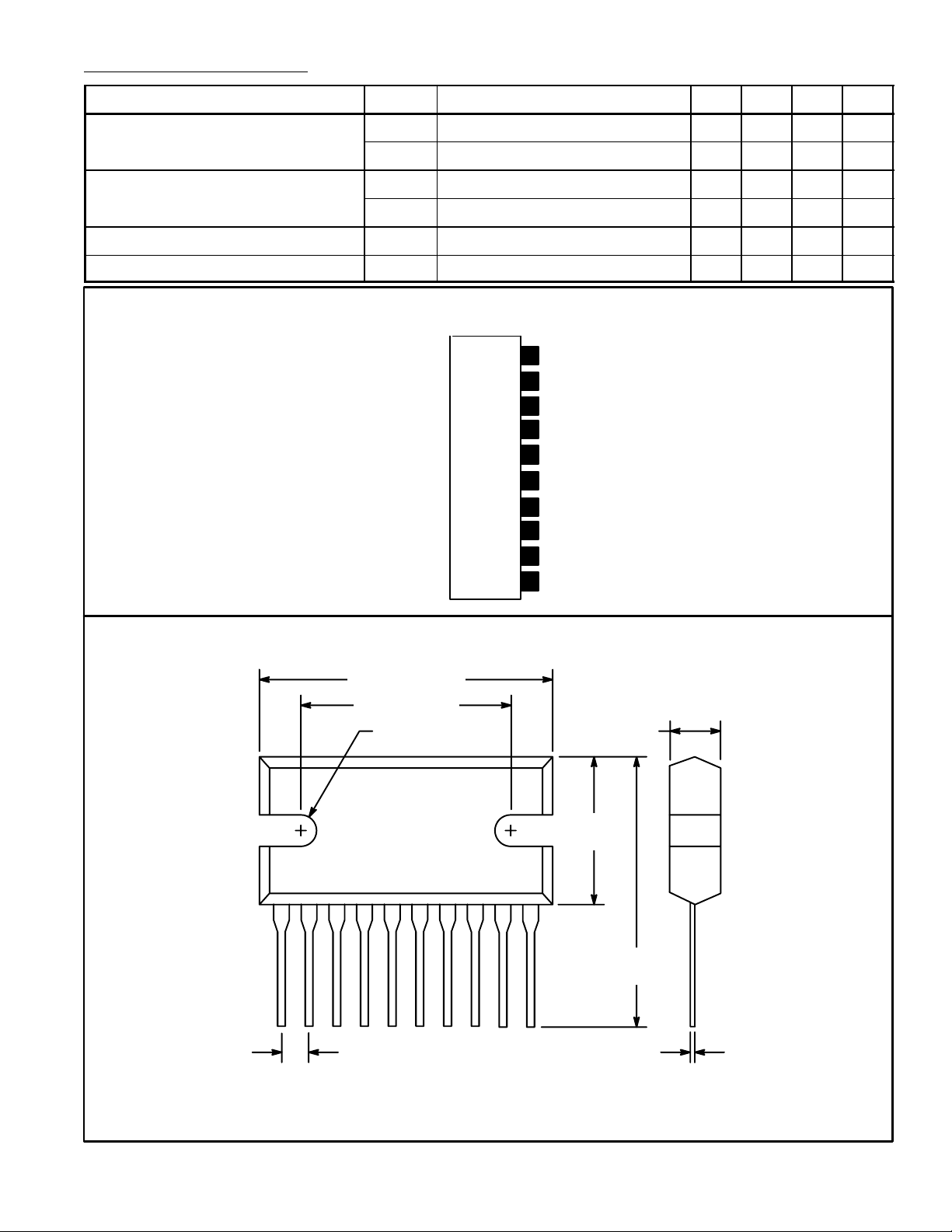
Pin Connection Diagram
(Front View)
N.C.
10
Pump–Up Output
9
V
8
OSC Stop
7
Input
6
Vert Output V
5
Vert Output
4
GND
3
N.C.
2
N.C.
1
– 0.5 1.0 V
– 1.8 2.6 V
– – 1.5 V
– 0.8 1.6 V
8.0 11.5 24.0 mA
– 11 – V
CC
CC
1.062 (27.0)
.788 (20.0)
.156 (3.95) R .157 (4.0)
.448
(11.4)
110
.740
(18.78)
.100 (2.54) .016 (0.40)
 Loading...