

NTE NTE1794 Datasheet
NTE1794
Integrated Circuit
Volatge Controlled Amp (VCA)
for dbx Noise Reduction System
Description:
The NTE1794 is a dbx noise reduction system voltage controlled amp (VCA) in an 8–Lead SIP type
package designed for use in tape decks and other audio equipment. This device features excellent
linearity VCA for wider input level due to super low noise and a high gain NPN/PNP complementary
process.
Features:
D Wide Operating Supply Voltage
D Excellent Linearity Control Constant
D Low Total Harmonic Distortion
D Low Noise
Absolute Maximum Ratings:
Supply Voltage, V
Supply Current, I
Power Dissipation (T
, V
CC
CC
= +75°C), P
A
EE
Operating Temperature Range, T
Storage Temperature Range, T
(TA = +25°C unless otherwise specified)
D
opr
stg
Recommended Operating Conditions:
Parameter Symbol Test Conditions Min Typ Max Unit
Operating Supply Voltage VCC, V
Bias Current I
Input Level Range υ
Note 1. I
= VEE – 4 VBE/R
SET
EXT
SET
in
= VEE – 2.4/R
–20° to +75°C. . . . . . . . . . . . . . . . . . . . . . . . . . . . . . . . . . . . . . . . .
–40° to 125°C. . . . . . . . . . . . . . . . . . . . . . . . . . . . . . . . . . . . . . . . . . .
Note 1 ±4 ±12 ±15 V
EE
– 2.0 – mA
–40 – +10 dBV
= 2mA
EXT
15V. . . . . . . . . . . . . . . . . . . . . . . . . . . . . . . . . . . . . . . . . . . . . . . . . . . . . . . . . . .
30mA. . . . . . . . . . . . . . . . . . . . . . . . . . . . . . . . . . . . . . . . . . . . . . . . . . . . . . . . . . . . . . .
330mW. . . . . . . . . . . . . . . . . . . . . . . . . . . . . . . . . . . . . . . . . . . . . .
Electrical Characteristics: (TA = +25°C, VCC = +12V, VEE = –12V, I
R
= R
IN
Parameter Symbol Test Conditions Min Typ Max Unit
= 33kΩ unless otherwise specified)
OUT
= 2mA, f = 1kHz,
SET
Supply Current I
Equivalent Input Bias Current I
Gain Cell Idling Current I
Gain Cell Offset Voltage V
Control Constant V
Total Harmonic Distortion THD AV = 0dB, VO = 0dBV, BPF = 400Hz to 5kHz – 0.007 0.07 %
Output Noise Level NV AV = 0dB, RIN = 33kΩ, BPF = 10Hz to 20kHz – –94 –84 dBV
Symmetry Control Voltage V
CC
IN
DLE
OFF
SYM
Non Signal 1.0 2.0 3.0 mA
Non Signal – 6 20 nA
Non Signal – 20 – µA
AV = 0dB, THD ≤ 0.07% – ±0.5 – mV
AV = –30dB to +30dB –5.8 –5.9 –6.1 mV/dB
C
AV = +20dB, VO = 0dBV, BPF = 400Hz to 5kHz – 0.02 0.10 %
AV = –20dB, VIN = 0dBV, BPF = 400Hz to 5kHz – 0.02 0.15 %
AV = 0dB, THD ≤ 0.07% –4 0 +4 mV
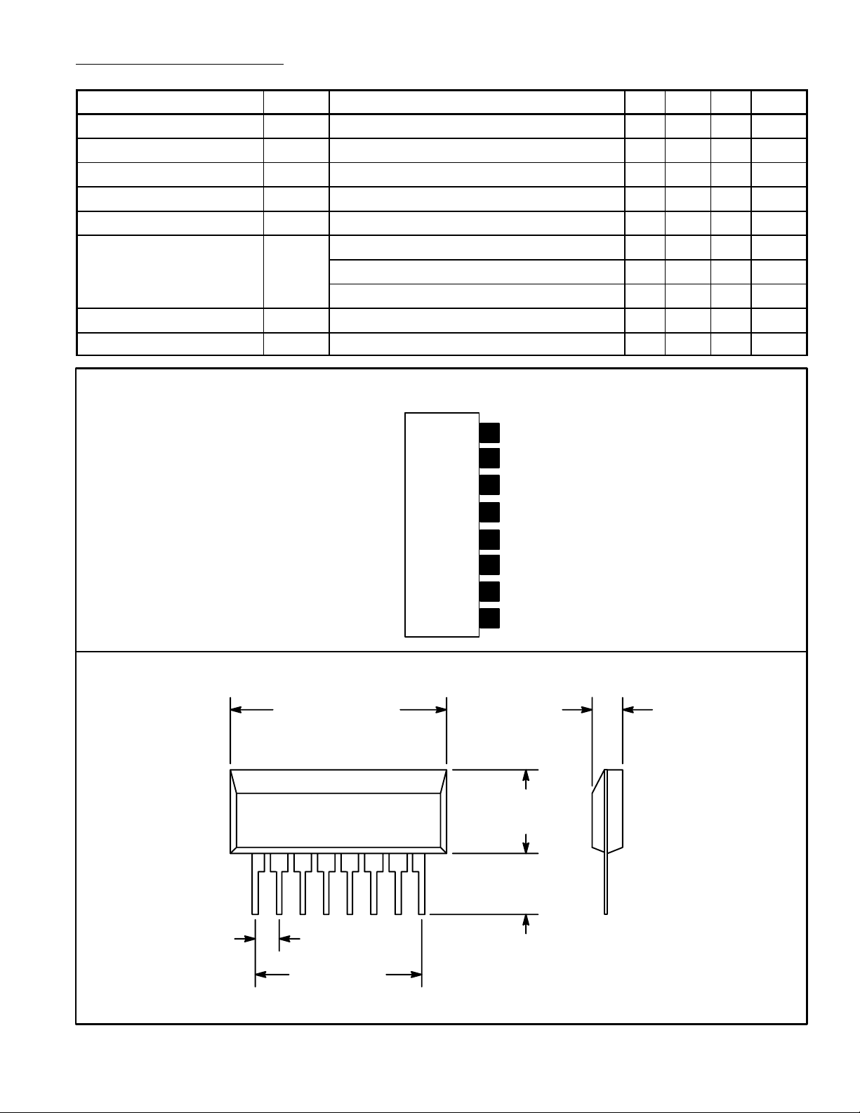
Pin Connection Diagram
(Front View)
8
Signal Output
7
V
CC
6
GND
5
I
SET
4
GC Bias
GC
3
2
1
.768 (19.52) Max
18
.100 (2.54) Typ
.118 (3.0) Max
1
GC
2
Signal Input
.264 (6.72)
Max
.165 (4.2)
Min
.700 (17.78)
 Loading...